- Center of Excellence in Nanotechnology at AIT
-
Center of Excellence at AIT 
CoEN @ AITMotto There is no sky to limit us at the bottom Type Center of Excellence Endowment NANOTEC, NSTDA Director Prof. Joydeep Dutta Academic staff 6 Admin. staff 5 Students 23 Postgraduates 23 Doctoral students 11 Location Klong Luang, Bangkok, Pathum Thani, Thailand Campus Suburban Website http://www.nano.ait.asia 
The Center of Excellence (CoE) in Nanotechnology is located inside the Asian Institute of Technology campus. It is one among the 8 Centers of Excellence in Thailand.
The CoEN at AIT is about applied research and graduate education in the newly emerging field of Nanotechnology. The unifying concept in the center's research activities is to make use of inexpensive wet-chemical methods to fabricate innovative materials and futuristic device components. Current research activities at the CoEN focuses on dye-sensitized solar cells, piezotronic devices, gas sensors, bio-diagnostic tools, specific microbial sensors, heavy metal ion sensors for waste water, environmental mitigation through visible light photocatalysis, self-organisation of nanoparticles, and layer-by layer growth from colloidal particles, among others. Master's degree program in Nanotechnology has been launched in 2009. The center has over 30 members from 10 different countries who are carrying out cutting-edge cross-disciplinary research in Nanotechnology.
Notable international collaborations are with: State University of New York, Buffalo, USA;[1] S N Bose National Centre for Basic Science,[2] India; Center of Photoelectrochemical Energy, Korea University, Jochiwon, South Korea;[3] Center for Nanobioscience, Agharkar Institute, India;[4] Inorganic Materials Laboratory, Royal Institute of Technology, Stockholm, Sweden; Swiss Federal Institute of Technology, Switzerland;[5] Uppsala University, Sweden;[6] University of Quebec, Canada;[7] Leibniz Institute of New Materials, Germany; University of California, Berkley, USA;[8] and Griffith University, Australia.[9]
History
 Prof. Joydeep Dutta,[10] Director, CoEN
The Center of Excellence in Nanotechnology was started in 2006 with an aim to address the creation of knowledge in areas relevant to Thailand, its industries and its people. Activities include joint research with other local and international universities and institutes, education and training personnel in the field of nanotechnology, technology transfer and promotion of public and industrial awareness of nanotechnology. This center provides international platform for academicians and researchers from Thailand, AIT and our partnered universities worldwide to work together in partnership with the industries.
In Thailand, there are currently 8 Centers of Excellence under Thailand National Nanotechnology Center: NANOTEC: CoE Kasetsert University, Bangkok; CoE Chulalongkorn University, Bangkok; CoE King Mongkut Institute of Technology Ladkrabang, Bangkok; CoE Mahidol University, Bangkok; CoE Asian Institute of Technology, Pathum Thani; CoE Prince of Songkhla University, Phuket; CoE Khon Kaen University, Khon Kaen; and CoE Chiang Mai University, Chiang Mai.
The Center of Excellence in Nanotechnology at AIT was set up, jointly with the National Nanotechnology Center, Thailand of the NSTDA,[11] at the Asian Institute of Technology campus, Thailand. Under the agreement, AIT and NANOTEC supports the center jointly. A few faculties at AIT joined hands to propose for this center to be established in the institute. The faculties came from all the three schools and the founding members were: Prof. Joydeep Dutta,[10] Prof. W. Kanok-Nukulchai,[12] Dr. Oleg Shipin,[13] Late Dr. N. Coowanitwong,[14] Dr. M. Parnichkun,[15] Dr. Mousa M. Nazhad,[16] Dr. S. Venkatesh[17] and Dr. P. Herabat.[18] A few rooms in the Chalarm Prakiat Building in Asian Institute of Technology were allocated for its operation. Initially, due to the lack of sufficient funds the center had a hard time to start performing. Prof. Joydeep Dutta,[10] CoEN Director, recalls, "I used to get glasses and mugs from my house to fulfill the students requirements for glasswares in the lab." Over the years the center got crowded with new equipments coming in and more researchers joining the nano-team. Eventually in September 2009, the center was officially shifted to the Outreach building.
On 8 September 2009, a state-of-the-art facility of the Center of Excellence in Nanotechnology at AIT was jointly inaugurated by Prof. Said Irandoust,[19] AIT President, and Dr. Paritud Bhandhubanyong,[20] Director, National Metal and Materials Technology Center.[21] The lab had bigger and larger space and was more free for the visitors from outside.
Administration
The Asian Institute of Technology governs the administrative activities of the Center of Excellence in Nanotechnology. Prof. Joydeep Dutta,[10] is the director of CoEN.
Campus
The facilities provided for the students in AIT is freely available to the researchers and students of the center. With a clean and green campus and sporting facilities such as football grounds, tennis fields, badminton, volleyball, basketball courts, a swimming pool, a golf course etc., the students can find time for recreation and physical workouts within the campus. A two-storied library is accessible to all the members of AIT.
Academics
Doctoral research in Nanotechnology was taking place since 2003. But, Master’s degree program in Nanotechnology at AIT was recently launched in August 2009.[22] It has attracted considerable interest amongst students across Asia. The program is open to graduates with Bachelor of engineering (electrical, chemical, mechanical, industrial, telecommunications, computer engineering, electronics, and instrumentation) as well as Bachelor of Science (physics and chemistry).
Essential features of AIT’s Nanotechnology degree program are: programmatic balance; processing nanostructures properties applications (P-N-P-A); interdisciplinarity; science (including biology) and technology; integrated classroom-lab experience; hands-on experiments and use of instrumentations; curriculum linked to applications; balance between theory and practice (industrial needs); and content addressing societal impact: public safety, ethics, and awareness.
Courses offered
The aim of the ‘integrated Master’s Degree programme in Nanotechnology’ is to address the knowledge-based industries of the 21st century that will require continuous development of their workforce in this new field as well as a technically updated management. The Nanotechnology course is designed in such a way that students from different disciplines can get easily acquainted with the subject matter. Prof. Dutta, Director, CoeN at AIT, and Prof. G. Louis Hornyak,[23] visiting faculty, are teaching students from different backgrounds such as Material sciences, Chemistry, Physics, Agriculture etc. The Nanotechnology Master’s Degree program is designed to be multidisciplinary covering areas such as:
- The macroscopic and microscopic world
- Physics/electronics
- Chemistry/chemical engg.
- Biotechnology
- Material sciences
- Microsystem Technology
- Instrumentation
- Environment
The list of the courses offered under School or an Institute-Level course: School of engineering and Technology and Area/Field of Study: Nanotechnology in AIT website[24] is given below:
- Self Assembly and molecular manufacturing (January)
- Impact of Nanotechnology on the Society (August)
- Intellectual Property Rights for Technology Development and Management (August)
- Solid State Physics for Nanotechnology (January)
- Fundamentals of Chemistry (August)
- Catalysis (August)
- Nano Thermodynamics (January)
- Nanomaterials and Nanotechnology (January)
- Colloids and Nanoparticles (August)
- Microelectronics Fabrication Technology (August)
- Microelectromechanical and Nanoelectromechanical systems (January)
- Characterization Tools in Nanotechnology (January)
- Advanced Seminars in Nanotechnology (January)
Admissions
Application for admissions to Master's degree in Nanotechnology can be made online or by mail by visiting the AIT website.[25] Application for admission takes only four steps:
- Step 1: Review Requirements and Procedures[26]
- Step 2: Download Application Forms[27]
- Step 3: Study Guidelines for Applicants[28]
- Step 4: Explore Financial Aid[29]
Research
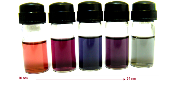
 Optical photos of Gold NPs between 10 – 24 nm in size
The Center of Excellence in Nanotechnology has acquired synthesis experience of nanoparticles by reactive precipitation techniques. Gold, silver, platinum, palladium, zinc sulphide, zinc oxide and silica nanoparticles are synthesized regularly at the center for a variety of applications. The platform technology of the center can be discussed as follows:
- Nanoparticles: gold, silver, platinum, paladium, silica, zinc oxide, zinc sulphide
- Nanowires: zinc oxide
- Coating Techniques: sol-gel coating, pyrosol coating, layer by layer organization, Ink-Jet printing, spin coating
 Micrographs of Au & Ag NPs. (a) Au10, (b) Au25, (c)Auai, (d) Ag10, (e) Ag25, and (f) Agai
The research efforts in AIT center are broadly classified into three groups:
- Environment: photocatalysis, heavy metal ion sensors, bacteria sensing, self-cleaning windows
- Agriculture and Food: E. coli sensors, E. nose, smart pesticides, gas sensors
- Alternate Energy Harvesting: nano-bio solar cells, nano-energy generators
Primary objective of the center is to seek applications of nanoparticles. Research work has extended to nanowires and extensive work is being carried out especially in the environmental application and the energy harvesting side for the application of nanowires on zinc oxide. The competence achieved at the CoEN in AIT has been primarily in the synthesis of metal nanoparticles like gold, silver, platinum and palladium, and zinc compounds namely zinc oxide and zinc sulphide. Some additional work on the development of sol-gel type titanium dioxide has also taken place. Doping of semiconductor nanoparticles and studies on the defect engineering of metal oxides have been another key area of research at the center with an objective to apply the added value obtained from defect engineering into some applications.
Synthesis of Nanoparticles
The different methods employed to synthesize nanoparticles of gold, silver, zinc sulphide, zinc oxide, silica among other is briefly given below:
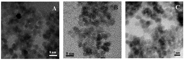
 TEM micrographs of the NPs synthesized in (A) isopropanol, (B) methonal, and (C) ethanol
Gold Nanoparticles
Generally, gold nanoparticles in aqueous solutions are synthesized by the reduction of hydrogen tetrachloroaurate (HAuCl4). To prevent the particles so formed from aggregating, often stabilizing agents are added. During the process, tri-sodium citrate reduces the gold salt to metallic gold particles, which acts as seeds for continuous growth.
SIlver Nanoparticles
 (A) HRTEM image showing ZnS:Mn2+ NPs of size between 4 to 6 nm. Crystallites are around 2 to 3 nm. (B) Fast Fourier Transform done on the squared area (C) Particle size distribution (100 particles sampled)
The silver nanoparticles are synthesized by chemical reduction of silver nitrate. The reducing reagent used for the synthesis of silver nanoparticles are similar to the Turkevitch method, i.e. using tri-sodium citrate. After creation of nanoparticle colloid, in order to increase the viscosity for jetting the inks, polymers such as Chitosan, Poly Vinyl Alcohol (PVA) and Poly Ethylene Glycol (PEG) are added to stabilize the solution.
ZnS Nanoparticles
 CS view of ZnO NRs grown by hydrothermal processes for different times
The organometallic synthesis of ZnS:Mn2+ nanoparticles developed is similar to the method described by Bhargava et al.
ZnO Nanoparticles
ZnO nanoparticles are synthesized in three different solvents and their optical absorptions studied to determine in which solvent the nanoparticles absorb maximum visible light in the optical band ranging between 400 nm and 700 nm. The nanoparticles synthesized in different solvents (isopropanol, methanol and ethanol) by the standard methods as explained in the experimental section yielded nanoparticles which are almost comparable in size (5 to 7 nm).
Silica Nanoparticles
Silica nanoparticles can be synthesized by sol-gel method - Stöber et al. published process for synthesize silica particles by hydrolysis of tetraethyl orthosilicate (TEOS) in ethanol solution - which is catalyzed by ammonia (NH3). Monodispersed silica spheres can be achieved from hydrolysis and condensation of alkoxide silicon by the following methods:
Hydrolysis: to form silanol groups
- Si(OR)4 + H2O → Si(OH)4 + 4(R-OH)
Condensation : to form siloxame bridges
- 2Si(OH)4 → 2(Si-O-Si) + 4H2O
 SEM micrographs showing the anisotropic ZnO NPs
ZnO can be synthesized to various novel structures due to loose pack of tetrahedral structures, different ionic radii of Zn2+ (74 pico m) and O2- (140 pico m). This causes large open spaces inside the hexagonal ZnO structure and makes it possible to control the shape of nanostructured particles. The growth of ZnO structures depend on various conditions, for example, pH of solvent, temperature, duration of growth as well as nature of solvent.
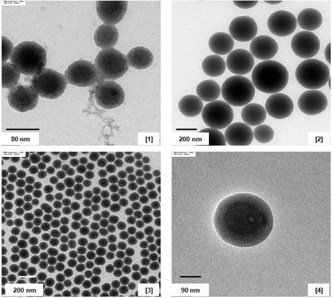
 TEM images of SiO2 NPs synthesized by Stoeber method
 TEM microraphs showing the silica coated anisotropic ZnO NPs
Besides concentration effect on particle size, it can also affect particle shape. Study from Masuda et al., synthesizing ZnO nanoparticles from zinc acetate [Zn(CH3COO)2] and ammonia precursors, shows that morphology of ZnO crystals was controlled by ratio of ammonia to zinc acetate NH3:Zn. This alters the super-saturation point of crystallization. The reaction is demonstrated in Figure .
Zinc acetate [Zn(CH3COO)2] solution is prepared in ethanol under vigorous stirring until zinc acetate is dissolved in ethanol in temperature around 50°C. Then ethanol is added and continuously stirred under temperature around 80°C for half an hour. After that, the solution is cooled under room temperature. NaOH in ethanol solution is prepared by vigorous stirring with 50°C, and then added to prepared zinc acetate in ethanol at room temperature. After that ZnO seeds are put in hexamethylenetetramine (HMT) solution, commonly called hexamine, for growth process. Hexamine is water soluble chemical and the growth process can be done in the temperature range 55-95°C. After ZnO nanopatilces are grown to desired shape, then the particles will be coated with silica particles by using Stoeber method. The process is carried out in ammonia-catalyzed reaction of TEOS in ethanol-water solution. Polyvinylpyrrolidone (PVP) can be added optionally for stabilization purpose. Hydrolysis reaction is initiated to form silica nanoparticles coated on ZnO nanoparticles.
ZnO Nanorods
The center is studying hydrothermal growth process of ZnO nanorods for the last few years. A typical process was carried out in a sealed chemical bath containing an equimolar solution of zinc nitrate hexahydrate and hexamethylene tetramine at a temperature of 95°C for a period of up to 20 hours. The thickness and length of the nanowires can be controlled by using different concentrations of the starting reactants and growth durations. A 0.5 mM chemical bath yielded nanowires with an average diameter of around 50 nm while a 25 mM bath resulted in wires with a thickness of up to about 1μm. The length of the wires depends both on the concentration of the precursor solution as well as the growth duration, and in 20 hours, nanowires as long as 10 µm can be grown.
This center has considerable experience in the fabrication of ZnO nanorods, nanowires, and nanotubes. ZnO nanoplates that are now being used for specific applications. We have acquired considerable expertise over the last years on the control of the aspect ratio and spacing of ZnO nanorods. Recently ink-jet printing was used to make arrays of ZnO nanorods.5
Applications of Nanoparticles
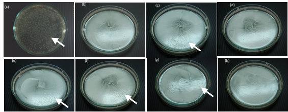
Antimicrobial property of an indoor paint containing silver nanopartilces on Escherichia coli
 Effect of antibacterial paint on E. coli
The antimicrobial property of silver colloid and water-based paint embedding silver nanoparticles (AgNPs) on Escherichia coli (E. coli) were studied. Silver colloid was synthesized by method proposed herewith showed the effective inhibited growth of E. coli with the concentration as low as 1ppm (parts per million) could completely stop the growth at E. coli concentration above 27ppm. Further the colloids were blended with the commercial water-based paint leading to formulation of an antimicrobial paint. After adding AgNPs the paints were stable for more than a month and no change in color was observed. The paint embedded with AgNPs showed the bactericidal effects, which is similar to silver colloids. The process to add AgNPs into the paint was simple and it was possible to integrate the current paint production lines.
 Reduction of viable cell counted percentage of paint embedding AgNPs
Because paint is a mixture of organic compounds, which can alter size and shape of AgNPs, some nanoparticle colloids cannot be compatibly mixed with paints. The important parameter for dispersing nanoparticles in the paint is stability of nanoparticles colloid, i.e. direct application of the zeta potential of the charged surface of nanoparticles and the pH of paint and colloid. Although the paint's recipe was modified by adding AgNPs colloids, the antimicrobial paints were stable for more than a month at room tempersture. This is because the paint and silver colloid have comparable pH and because the adding volume was small due to the high concentration of the colloid. The pH of paint was more than 10 and the pH of the silver colloid was about 9 to 10 with zeta potential of ~50mV (milliVolt). Then, AgNPs paints were tested on antimicrobial property in order to show that the AgNPs can perform the same or better as in the colloidal form. And it turned out, the AgNPs paint showed antimicrobial property in the same way as in the colloidal form. Moreover, the inhibition of AgNPs containing paints was higher than the silver colliod due to possibly the inhibition of paints itself. In all experiments, the thickness of paint layer was minimized in order to allow bacteria to access the air. The percentage of viable cells reduced as the concentration of AgNPs in paints increased. The number of CFU (colony forming units) reduced significantly with increase in the concentration of AgNPs in paint loading 0.5ppm and higher. The optical image of cultured plates recorded after incubation showed that the paints preserved the original color and texture.
Highly efficient zinc oxide nanorod dye sensitized solar cell
 Fig. 1: FESEM image of cross sectional view of the ZnO NRs grown by the hydrothermal process at 90°C. Inset shows the top view of the ZnO NRs
ZnO nanorods grown via hydrothermal process have been used successfully as photoelectrode materials in dye-sensitized solar cells (DSSC). Such one-dimensional nanorods offer a direct conduction pathway for electron transport in the solar cell. Cell performance was evaluated from measurements of open-current voltage (Voc), short-circuit current density (Jsc), fill factor (FF), and quantum efficiency (η) vs. annealing temperature. ZnO nanorods annealed at 350°C showed the best overall performance.
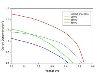
 Fig. 2: I-V characteristics of DSSC with ZnO nanorods photo electrode annealed at various temperature (active area is 1 cm2)
Figure 1 shows the field emission scanning electron microscopy (FESEM) image of highly dense hydrothermally grown ZnO nanorods on FTO substrates. The I-V characteristic of the DSSC measured under 100 mW/cm2 solar radiation with ZnO nanorods annealed at various temperatures are shown in figure 2. The maximum device performance was obtained at annealing temperature of 350°C.
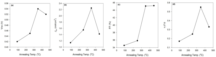
In figure 3, the variation of the DSSC parameters with annealing temperature are shown.
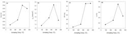 Fig. 3: Variation of DSSC parameters with annealing temperature (a) Voc, (b) Jsc, (c) FF and (d) η
The open circuit voltage (Voc) of a DSSC is the difference between the Fermi energy of the semiconductor (ZnO in this case) and redox potential of the electrolyte. The position of the Fermi level changes due to the electron accumulation in the conduction band (CB) of the ZnO. For defective nanorods, the injected electrons from dye to CB of ZnO quickly recombine in the defect sites and hence the electron density in the CB of the ZnO becomes less for defective rods. This results in a low Voc as shown in figure 3(a). As the defect sites are removed by annealing at different temperatures (250°C, 350°C and 450°C), improvement in Voc was observed (figure 3(a)). But at higher annealing temperature of 450°C, due to the removal of sufficient surface defects, a decrease in Voc was observed. Fewer defects in this case lead to less dye adsorption, which resulted in less electron injection to the conduction band (CB) of ZnO and thus lowered electron accumulation. A similar case was observed for the short circuit current density, Jsc (Figure 3(b)). For defective ZnO nanorods, due to electron recombination, lower Jsc were observed. The maximum Jsc was obtained at an annealing temperature of 350°C. At 450°C, there was less dye adsorption, and as a result, lower Jsc was measured. The FF of the DSSC also improved with higher annealing temperature. The maximum conversion efficiency was obtained for ZnO nanorods annealed at 350°C.
Self assembly of gold nanoparticles with chitosan/PDDA encapsulated silica colloidal nanoparticles
 Optical Absorption Spectra of multilayer thin films of Silica and Gold showing higher absorbance with (a) increased dip time (b) increase in number of multilayers
The templated growth of organic, inorganic and hybrid networks involving self-assembly with organogels, using tuned parameters, enables us to develop innovative nanostructures. In this research work, different strategies are employed to fabricate thin films using colloidal nanoparticles of metal and insulator materials, capped with organic polymers to provide stability and electrostatic binding forces to build heterogeneous devices.
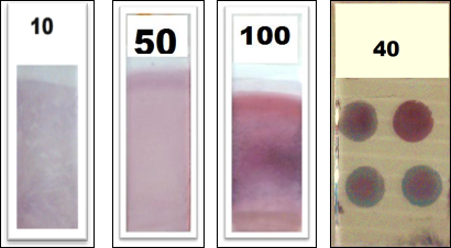
 From left to right: 10 Bi-Layers, 50 Bi-Layers, 100 Bi-Layers, and 40 Bi-Layers of CTS capped Silica & Gold
Measurements carried out over various substrates showed repeatable optical characteristics thus demonstrating the uniformity of the deposition process. The average sizes used for the experiments of gold and silica nanoparticles were 20 nm and 100 nm, respectively. The wettability of the glass slides was studied using contact angle measurements utilizing the sessile drop method with ultra pure water as shown in figure 17. A drop of DI water (5 μL) was placed onto the glass surface. Mean water contact angle (WCA) of the annealed glass slides were measured to be 11.9° taken through a DinoLite microscopic camera thus showing that annealing at high temperature helped to increase the hydrophilicity of the glass substrate which can improve the attachment of the first layer of electrolyte solution. Scanning Electron Microscopy (SEM) was performed. The image in figure 18 shows the thickness of the multilayers being grown. Varying the dip, dry and wash times from 5 minutes to 10 minutes resulted in an increase in the absorbance values of nanoparticles as seen in the optical absorption spectroscopy (figure 19). The peak absorption values for both the Silica NPs and Gold NP s measured at wavelengths of 320 nm and 520 nm confirmed the presence as well as the uniform deposition for the both.
Defect engineering of zinc oxide nanorods for visible light photocatalysis
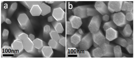
 Scanning electron micrograps of zinc oxide nanorods prepared through (a) conventional method (b) fast crystallization
Toxic wastes from industries are ceaselessly polluting the environment and urgent efforts are needed for the removal of harmful contaminants from soil and waste water. Wide band gap metal oxide semiconductors like zinc oxide (ZnO) exhibit photocatalytic properties that have been exploited to degrade harmful organic contaminants into benign fragments like mineral acids. Photocatalysis is a process by which free radicals are generated in the presence of light, through the creation of electron-hole pairs that are capable of breaking up complex organic molecules. Metal oxides show enhanced photocatalytic activity with the increase in surface defects in the crystals as this can alleviate electron hole separation.
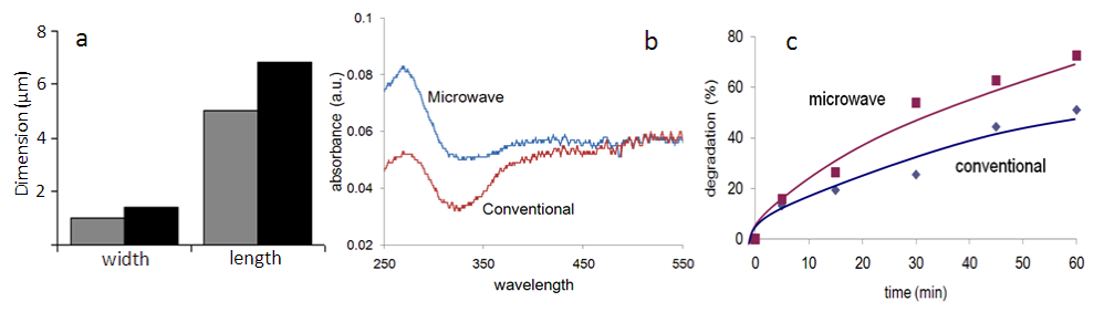
 (a) Comparison of the width and length of ZnO nanorods grown through conventional and fast crystallization methods; grey:conventional; black:microwave (b) fast crystallized nanorods showing higher absorption in the visible region (c) increased degradation of MB using microwave synthesized ZnO nanorods
A commonly used method of incorporating defect sites or electron vacancies into the ZnO crystal is through doping using transition metals like manganese, iron, cobalt, etc. However, the center have successfully created crystal defects by controlling the crystallization process during the growth of ZnO nanoparticles. This was possible through rapid nucleation and growth of the crystals followed by immediate quenching of the precipitation reaction. ZnO normally absorb electromagnetic waves in the ultra violet region below 370 nm (Eg= 3.37eV), but by introducing defects into its crystal lattice, a shift in the optical absorption towards the visible light band (400 nm to 700 nm) was observed. An increase in photocatalytic activity was observed due to the creation of intermediate states that inhibits photogenerated electron hole recombination, allowing redox reactions.
One dimensional nanostructures of zinc oxide like nanowires, nanorods, etc. are ideal photocatalysts because of large surface to volume ratio and inherent surface defects. Increasing the surface defects through rapid crystallization increases the optical absorption in the visible region (λ: 400-700 nm) and showed improved photocatalytic degradation of methylene blue upon illumination with white light.
Photocatalysis test was performed using a test contaminant, methylene blue [C16H18N3SCl] (MB) which is a heterocyclic aromatic compound, in aqueous solution. Photocatalytic degradation of (MB) results in the formation of colourless leuco methylene blue (LMB) [4]. A 10 μM solution of MB in water was put in cuvettes along with the glass slide containing ZnO nanorods. The cuvettes are placed in front of a halogen light source (500W). 72 klux of light at the sample position was measured by a luxmeter calibrated to 550 nm wavelength. Optical absorption spectra were taken after different time durations using an Ocean Optics spectrophotometer to monitor the rate of decolorization of the test contaminant. The degradation of the dye was estimated in terms of the change in intensity at λmax(~665 nm) of MTC. The degradation efficiency is calculated using the expression, where I0 is the initial absorption intensity of MTC at λmax= 665 nm and I the intensity after photoirradiation. C0 is the initial concentration of the dye and C is the concentration after photoirradiation. Figure shows the scanning electron micrographs of the ZnO nanorods grown using the conventional method and through microwave irradiation. Structural defects on the polar face are clearly visible for the fast crystallized nanorods. Figure 20(a) shows that ZnO nanorods grown using 10mM growth concentration under microwave irradiation for 5 hours were wider (40%) and longer (36%). Figure 20(b) shows that the ZnO nanorods grown through fast crystallization have higher optical absorption in the visible region of the electromagnetic spectrum as compared to the conventionally synthesized ones. This higher visible light absorption is indicative of the creation of mid band quasi-stable defect states to which valence band electrons can be excited with energy as low as 2.75eV. The photocatalytic degradation of MB was observed up to 60 minutes light exposure as detailed in the experimental section. In this experiment we fixed all parameters like sample size, effective surface area available for contaminant adsorption (34.27 cm2 for the conventional sample and 33.74 cm2 for the fast crystallized one), intensity of irradiated light (72klux) and duration of photonic exposure (60 minutes) almost similar. The comparative results are shown in Figure 20(c). It is interesting to observe that the microwave synthesized nanorods showed better photocatalytic activity as compared to the conventionally synthesized rods. This is attributed to the higher density of electron deficient sites when faster growths of the crystals were imbibed by using microwaves. These sites can trap photogenerated electrons and reduce recombinations thereby improving the photocatalytic activity.
News
August 2010
 Introducing the younger generation to the fascinating world of Nanotechnology
9 August 2010: National Science and Technology Fair 2010 (NSTF 2010):
Center of Excellence in Nanotechnology at AIT got actively involved in designing and conceptualizing the Nanotechnology Pavilion at National Science and Technology Fair 2010 being held until 22 August 2010 at Bangkok International Trade and Exhibition Center (BITEC), Bang-na, Bangkok.
File:Nanonews NSF02.JPGArray of Fluorescent Quantum Dots displayed at the Nanotechnology PavilionWith this year’s slogan “Towards a better society with Science and Technology,” the National Science and Technology Fair 2010 was formally inaugurated by Dr. Virachai Virameteekul, Minister of Science and Technology, Thailand, on 7 August 2010. The fair covered a total area of 42,000 sq. meters at the grounds of Bangkok International Trade and Exhibition Center (BITEC), Bang-na, Bangkok. With 7 ministries, 11 private enterprises, 5 major science societies, and 30 agencies from different universities participating from Thailand and more than 10 agencies participating from the overseas, it is the largest Science and Technology Fair held in Thailand. Around a million visitors, consisting of mainly school and university students from different parts of the country, are expected to visit the fair by its final day on 22 August 2010.
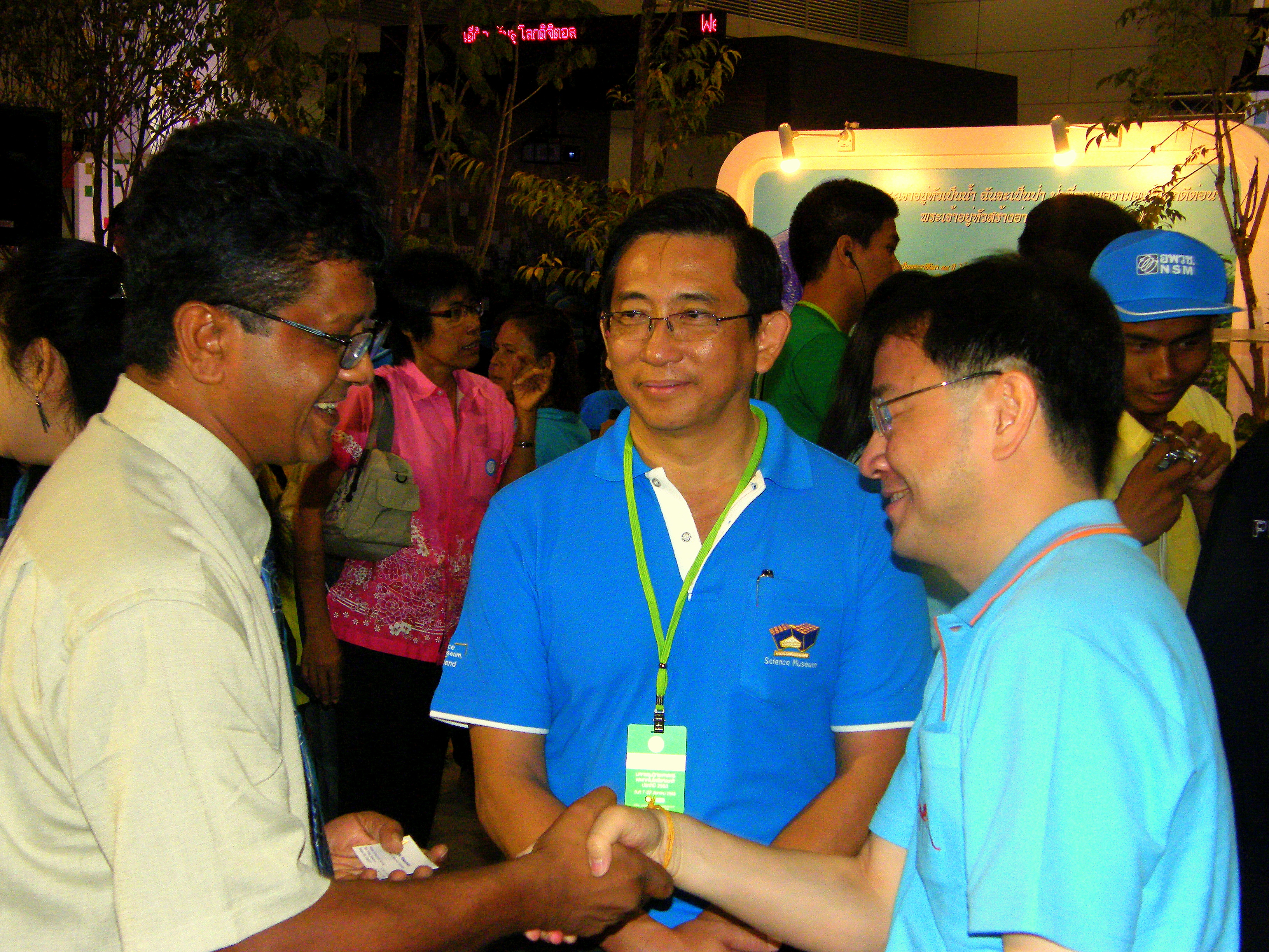
 Prof Joydeep Dutta, Director of CoEN at AIT and current Vice President- Academic Affairs, AIT (left) with Dr. Pichai Sonchaeng, President of National Science Museum of Thailand (middle) and Dr. Virachai Virameteekul, Minister of Science and Technology, Govovernment of Thailand (right) at the National Science and Technology Fair 2010
The participants were categorized into 9 exhibition and activity sections, namely Royal Pavilion, Ministry Pavilion, International Pavilion, University Pavilion, Science Associations, Private Enterprises, Thematic Exhibition, Activity for Youth Zones, and Academic Conference/Seminar/Workshop.
 Model showing section of NPs with the atoms aligned in the crystal
The Center of Excellence in Nanotechnology at AIT (CoEN at AIT), in collaboration with the National Science Museum, Thailand, helped in conceptualizing and designing the Nanotechnology Pavilion set up under the section: Thematic Exhibition. The exhibits at the pavilion, many of which were provided by CoEN at AIT, were designed to introduce the students to a whole new world of nanotechnology through simple demonstrations and hands-on activities. Children were busy with activities, such as making their own C60 fullerene (Bucky ball) model using magnetic legos, trying to understand surface to volume ratio increase with size minimization using building blocks, playing with model explaining nanostructures etc. For the more mature audience a variety of information in the form of video for explaining the concept of scale and for demonstrating ZnO-based LPG gas sensors etc. were provided at the Pavilion.
With the growing popularity of Nanotechnology in Thailand and, in many ways, due to the active involvement of Prof. Joydeep Dutta, the Director of CoEN at AIT and the current Vice President - Academics Affairs of AIT, in promoting Nanotechnology-based research in Thailand, it was small wonder to see students from various schools and colleges taking keen interest in, what many believe is, the technology of the future.
Publications
Over the past 6 years, the members of the center has published quite a few number of research papers in different journals. There are few books that were released in 2008 and 2009. A list of major publications from 2005 onwards is given below:
Books
- G. Louis Hornyak, Joydeep Dutta, Harry F. Tibbals and Anil K. Rao, 2008, Introduction to NanoScience, CRC Press of Taylor and Francis Group LLC (ISBN 14-2004-8058)
- G. Louis Hornyak, Joydeep Dutta, John J. Moore and Harry F. Tibbals, 2009, Fundamentals of NanoTechnology, CRC Press of Taylor and Francis Group LLC (ISBN 14-2004-8031)
- G. Louis Hornyak, Joydeep Dutta, John J. Moore and Harry F. Tibbals, 2009, Introduction to Nanoscience & Nanotechnology, CRC Press of Taylor and Francis Group LLC (ISBN 14-2004-7795)
Book Chapters
- Nanoparticle Applications for Environmental Control and Remediation,S. Baruah, Rungrot Kitsaboonloha, Myo Myint Zar and J. Dutta, Nanoparticles: Synthesis, Characterization and Applications Edited by R. S. Chaughule and R. V. Ramanujan, American Scientific Publishers, Valencia, California, USA, (2009), Chapter 12 (22 Pages), in Press
- Nanotechnology for Agriculture, Food Systems and the Environment, S. Baruah, S. L. Ranamukhaarachchi and J. Dutta, The Age of Nanotechnology (2009), ed. Nirmala Rao Khadpekar, The ICFAI University Press, Hyderabad, India, in press
- Nanomaterials for Energy Conversion Applications, V. Renugopalakrishnan, A. M. Kannan, S. Srinivasan, V. Thavasi, S. Ramakrishna, P. Li, A. Mershin, S. Filipek, A. Kumar, J. Dutta, A. Jaya, L. Munukutla, S. Velumani, and G. F. Audette, Nanomaterials for Energy Storage Applications, Ed. H. S. Nalwa, American Scientific Publishers, Stevens Ranch, CA, USA, Ch. 5, pages 155–178, 2008
- Pollution Treatment, Remediation, and Sensing, A. Sugunan and J. Dutta, Nanotechnology, Volume 2: Environmental Aspects (2008), Krug, Harald (ed.), Wiley-VCH, Weinheim, Germany- ISBN 978-3-527-31735-6, pg. 125-146
- Nanotechnology for Agriculture and Food Systems- A view, H. Warad and J. Dutta, The Age of Nanotechnology (2007), page 206-220, ed. Nirmala Rao Khadpekar, The ICFAI University Press, Hyderabad, India (ISBN 81-314-0828-0)
Recreation center - A Little Nano Band
After a hard weeks work, the Nano-group members enjoy a little recreation to ease of the stress and tension. With the initiatives of a visiting faculty to CoEN, Prof. Gabor L. Hornyak, Vice President, NanoThread, Inc.,[23] a small band named A little Nano Band was created. With professor himself on Bass or Piano, Bo Tay on rhythm guitar, Tanujjal Bora on Drums, Htet Kyaw on Tambourine and Ajaya Sapkota or Mayuree Jaisai on Vocals, the band plays covers of songs from 1960s classics to the present day pop music. The cultural diversity of the institution facilitates the band to select songs from different languages and play it to a vast group of listeners.
References
- ^ State University of New York, Buffalo, USA
- ^ S N Bose National Centre for Basic Science
- ^ Korea University: Research
- ^ Center for Nanobioscience, Agharkar Institute, India
- ^ Swiss Federal Institute of Technology, Switzerland
- ^ University, Sweden
- ^ University of Quebec, Canada
- ^ Vivek Subramanian, University of California, Berkley
- ^ Dr Denis Sweatman, Griffith University, Australia
- ^ a b c d Prof. Joydeep Dutta
- ^ National Science and Technology Development Agency: NSTDA
- ^ Prof. W. Kanok-Nukulchai
- ^ Dr. Oleg Shipin
- ^ Late Dr. N. Coowanitwong
- ^ Dr. M. Parnichkun
- ^ Dr. Mousa M. Nazhad
- ^ Dr. S. Venkatesh
- ^ Dr. P. Herabat
- ^ Said Irandoust
- ^ Dr. Paritud Bhandhubanyong
- ^ National Metal and Materials Technology Center, Thailand
- ^ Launch of Master's degree program in Nanotechnology at AIT
- ^ a b Prof. Gabor L. Hornyak, Vice President, NanoThread, Inc.
- ^ Course-catalog
- ^ Admissions to Nanotechnology
- ^ Review Requirements and Procedures
- ^ Download AIT Application Forms
- ^ Study Guidelines for Applicants
- ^ Explore Financial Aid
External links
Categories:


Wikimedia Foundation. 2010.