- Dip-pen nanolithography
-
Dip Pen Nanolithography (DPN) began as a scanning probe lithography technique where an atomic force microscope tip was used to transfer alkane thiolates to a gold surface. This technique allows surface patterning on scales of under 100 nanometers. DPN is the nanotechnology analog of the dip pen (also called the quill pen), where the tip of an atomic force microscope cantilever acts as a "pen," which is coated with a chemical compound or mixture acting as an "ink," and put in contact with a substrate, the "paper."
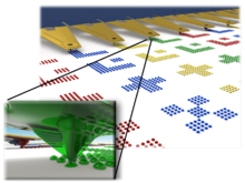
DPN enables direct deposition of nanoscale materials onto a substrate in a flexible manner. Recent advances have demonstrated massively parallel patterning using two-dimensional arrays of 55,000 tips. Applications of this technology currently range through chemistry, materials science, and the life sciences, and include such work as ultra high density biological nanoarrays, and additive photomask repair[1].
The uncontrollable transfer of a molecular 'ink' from a coated AFM tip to a substrate was first reported by Jaschke and Butt in 1995[2], but they erroneously concluded that alkanethiols could not be transferred to gold substrates to form stable nanostructures. A research group at Northwestern University led by Chad Mirkin studied the process and determined that under the appropriate conditions, molecules could be transferred to a wide variety of surfaces to create stable chemically-adsorbed monolayers in a high resolution lithographic process they termed "DPN" [3]. Mirkin and his coworkers hold the patents on this process, and the patterning technique has expanded to include liquid "inks". It is important to note that "liquid inks" are governed by a very different deposition mechanism when compared to "molecular inks".
Contents
Deposition materials
Molecular inks
 Classic DPN mechanism: Molecular ink diffusing from a nanoscale tip to a surface through a water meniscus.
Molecular inks are typically composed of small molecules that are coated onto a DPN tip and are delivered to the surface through a water meniscus. In order to coat the tips, one can either vapor coat the tip or dip the tips into a dilute solution containing the molecular ink. If one dip-coats the tips, the solvent must be removed prior to deposition. The deposition rate of a molecular ink is dependent on the diffusion rate of the molecule, which is different for each molecule. The size of the feature is controlled by the tip/surface dwell-time (ranging from milliseconds to seconds) and the size of the water meniscus, which is determined by the humidity conditions (assuming the tip's radius of curvature is much smaller than the meniscus).
- Water meniscus mediated (exceptions do exist)
- Nanoscale feature resolution (50 nm to 2000 nm)
- No multiplexed depositions
- Each molecular ink is limited to its corresponding substrate
Examples
- Alkane thiols written to gold
- Silanes written to glass or silicon
Liquid inks
 Liquid ink deposition mechanism
Liquid inks can be any material that is liquid at deposition conditions. The liquid deposition properties are determined by the interactions between the liquid and the tip, the liquid and the surface, and the viscosity of the liquid itself. These interactions limit the minimum feature size of the liquid ink to about 1 micrometre, depending on the contact angle of the liquid. Higher viscosities offer greater control over feature size and are desirable. Unlike molecular inks, it is possible to perform multiplexed depositions using a carrier liquid. For example, using a viscous buffer, it is possible to directly deposit multiple proteins simultaneously.
- 1-10 micrometre feature resolution
- Multiplexed depositions
- Less restrictive ink/surface requirements
- Direct deposition of high viscosity materials
Examples
- Protein[4][5], peptide[6], and DNA[7] patterning
- Hydrogels
- Sol gels[8]
- Conductive inks[9]
- Lipids[10]
Applications
In order to define a good DPN application, it is important to understand what DPN can do that other techniques can't. Direct-write techniques, like contact printing, can pattern multiple biological materials but it cannot create features with subcellular resolution. Many high-resolution lithography methods can pattern at sub-micrometre resolution, but these require high-cost equipment that were not designed for biomolecule deposition and cell culture. Micro contact printing can print biomolecules at ambient conditions, but it cannot pattern multiple materials with nanoscale registry.
Industrial applications
The following are some examples of how DPN is being applied to potential products.
 Cantilever biosensor functionalized with 4 different proteins
- Biosensor Functionalization - Directly place multiple capture domains on a single biosensor device
- Nanoscale Sensor Fabrication - Small, high-value sensors that can detect multiple targets[11]
- Nanoscale Protein Chips - High-density protein arrays with increased sensitivity
Emerging applications
Cell engineering
DPN is emerging as a powerful research tool for manipulating cells at subcellular resolution[12][13]
- Stem cell differentiation
- Subcellular drug delivery
- Cell sorting
- Surface gradients
- Subcellular ECM protein patterns
- Cell adhesion
Rapid prototyping
 SEM image of DPN fabricated gold metastructure arrays.
- Plasmonics and Metamaterials
- Cell and tissue screening
DPN properties
Direct write
DPN is a direct write technique so it can be used for top-down and bottom-up lithography applications. In top-down work, the tips are used to deliver an etch resist to a surface, which is followed by a standard etching process[14]. In bottom-up applications, the material of interest is delivered directly to the surface via the tips.
 Gold on silicon metastructure fabricated with top-down DPN methods
Unique advantages
- Directed Placement - Directly print various materials onto existing nano and microstructures with nanoscale registry
- Direct Write - Maskless creation of arbitrary patterns with feature resolutions from as small as 50 nm and as large as 10 micrometres[15]
- Biocompatible - Subcellular to nanoscale resolution at ambient deposition conditions
- Scalable - Force independent, allowing for parallel depositions[16]
Common misconceptions
Direct comparisons to other techniques
 Streptavidin (4nm thickness)deposited using micro contact printing
The criticism most often directed at DPN is the patterning speed. The reason for this has more to do with how it is compared to other techniques rather than any inherent weaknesses. For example, the soft lithography method, micro contact printing (μCP), is the current standard for low cost, bench-top micro and nanoscale patterning, so it is easy to understand why DPN is compared directly to micro contact printing. The problem is that the comparisons are usually based upon applications that are strongly suited to μCP, instead of comparing them to some neutral application. μCP has the ability to pattern one material over a large area in a single stamping step, just as photolithography can pattern over a large area in a single exposure. Of course DPN is slow when it is compared to the strength of another technique. DPN is a maskless direct write technique that can be used to create multiple patterns of varying size, shape, and feature resolution, all on a single substrate. No one would try to apply micro contact printing to such a project because the it would never be worth the time and money required to fabricate each master stamp for each new pattern. Even if they did, micro contact printing would not be capable of aligning multiple materials from multiple stamps with nanoscale registry[17]. The best way to understand this misconception is to think about the different ways to apply photolithography and e-beam lithography. No one would try to use e-beam to solve a photolithography problem and then claim e-beam to be "too slow". Directly compared to photolithography's large area patterning capabilities, e-beam lithography is slow and yet, e-beam instruments can be found in every lab and nanofab in the world. The reason for this is because e-beam has unique capabilities that cannot be matched by photolithography, just as DPN has unique capabilities that cannot be matched by micro contact printing.
Connection to Atomic Force Microscopy
DPN evolved directly from AFM so it is not a surprise that people often assume that any commercial AFM can perform DPN experiments. In fact, DPN does not require an AFM, and an AFM does not necessarily have real DPN capabilities. There is an excellent analogy with scanning electron microscopy (SEM) and electron beam (E-beam) lithography. E-beam evolved directly from SEM technology and both use a focused electron beam, but no one would ever suggest that one could perform modern E-beam lithography experiments on a SEM that lacks the proper lithography hardware and software requirements.
It is also important to consider one of the unique characteristics of DPN, namely its force independence. With virtually all ink/substrate combinations, the same feature size will be patterned no matter how hard the tip is pressing down against the surface[18]. As long as robust SiN tips are used, there is no need for complicated feedback electronics, no need for lasers, no need for quad photo-diodes, and no need for an AFM.
References
- ^ Solvent-mediated repair and patterning of surfaces by AFM: Elhadj, Chernov, De Yoreo, Nanotechnology, 19, (2008) 105304
- ^ Jaschke M.; Butt, H.-J. "Deposition of Organic Material by the Tip of a Scanning Force Microscope" Langmuir, 1995, 11, 1061-1064.
- ^ Piner, R. D.; Zhu, J.; Xu, F.; Hong, S.; Mirkin, C. A. "Dip Pen Nanolithography," Science, 1999, 283, 661-663
- ^ Protein nanoarrays generated by DPN: 1 March 2002 Vol 295 Science
- ^ Biologically Active Protein Nanoarrays Generated Using Parallel DPN: Adv. Mater. 2006, 18, 1133–1136
- ^ Dip-Pen Nanolithography of Bioactive Peptides on collagen-terminated retinal membrane: Sistiabudi and Ivanisevic, Adv. Mater. 2008, 20, 1–4
- ^ Direct Patterning of Modified Oligos on Metals and Insulators by DPN: 7 JUNE 2002 VOL 296 SCIENCE
- ^ Nanopatterning of “Hard” Magnetic Nanostructures via DPN and a Sol-based Ink: Fu, Liu, Zhang, Dravid Nano Letters, 2003, Vol. 3, No. 6, 757-760
- ^ Dip-pen nanopatterning of photosensitive conducting polymer using a monomer ink: Su, Aslam, Fu, Wu, Dravid, Appl. Phys. Lett., Vol. 84, No. 21, 24 May 2004
- ^ small 2008, 4, No. 10, 1785–1793
- ^ Preparation of gas sensors via DPN: Tang and Shi, Sensors and Actuators B, 131 (2008) 379-383
- ^ Surface Chemistry and Cell Biological Tools for the Analysis of Cell Adhesion and Migration: Pulsipher, Yousaf: ChemBioChem 2010, 11, 745 – 753
- ^ Model substrates for studies of cell mobility: Current Opinion in Chemical Biology 2009, 13:1–8
- ^ High-throughput DPN-based fabrication of Si nanostructures: Zhang, Amro, Disawal, Elghanian, Shile, Fragala Small, 2007, 3, No. 1, 81-85
- ^ http://en.wikipedia.org/wiki/Maskless_lithography
- ^ Nature Chemistry Vol 1, August 2009
- ^ Mei, Y., Cannizzaro, C., Park, H., Xu, Q., Bogatyrev, S., Yi, K., Goldman, N., Langer, R. and Anderson, D., Cell-compatible, multicomponent protein arrays with subcellular feature resolution, Small, 4: 1600-1604, 2008
- ^ Exceptions exist when printing to soft materials - J. of Applied Physics, 104, 014311 (2008)
See also
- Nanolithography
- NanoInk, Inc. DPN Instrumentation
- DPN based protein assay kits
- NanoProfessor, Hands-on nanotech education
Nanolithography Techniques Soft · Nanoimprint · Scanning probe · Local oxidation · Dip-Pen · Electron beam · Extreme ultraviolet · X-ray · Magnetolithography
See also Categories:- Lithography (microfabrication)
- Microtechnology
- Nanotechnology
- Bioengineering
- Tissue engineering


Wikimedia Foundation. 2010.