- Quad-flat no-leads package
-
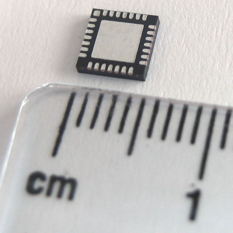
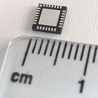 28-pin QFN, upside down to show contacts and thermal/ground pad
Flat no-leads packages such as QFN (quad-flat no-leads) and DFN (dual-flat no-leads) physically and electrically connect integrated circuits to printed circuit boards. Flat no-leads, also known as MicroLeadFrame, is a surface-mount technology, one of several package technologies that connect ICs to the surfaces of PCBs without through-holes. Flat no-lead is a near chip scale package plastic encapsulated package made with a planar copper lead frame substrate. Perimeter lands on the package bottom provide electrical connections to the PCB.[1] Flat no-lead packages include an exposed thermal pad to improve heat transfer out of the IC (into the PCB). Heat transfer can be further facilitated by metal vias in the thermal pad.[2] The QFN package is similar to the quad-flat package, and a ball grid array.
Contents
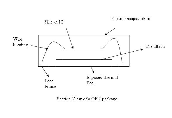
Flat No lead Cross section
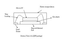 QFN sideview.
The figure shows the cross section of a Flat No lead package with a lead frame and wire bonding. There are two types of body designs, punch singulation and saw singulation.[3] Saw singulation cuts a large set of packages in parts. In punch singulation, a single package is moulded into shape. The cross section shows a saw-singulated body with an attached thermal head pad. The lead frame is made of copper alloy and a thermally conductive adhesive is used for attaching the silicon die to the thermal pad. The silicon die is electrically connected to the lead frame by 1-2mil diameter gold wires.
The pads of a saw-singulated package can either be completely under the package, or they can fold around the edge of the package.
Different Types of QFNs
Two types of QFN packages are common: air-cavity QFNs, with an air cavity designed into the package, and plastic-moulded QFNs with air in the package minimized.
Less-expensive plastic-moulded QFNs usually limited to applications up to ~2–3 GHz. It is usually composed of just 2 parts, a plastic compound and copper lead frame, and does not come with a lid.
In contrast, the air-cavity QFN is usually made up of 3 parts; a copper leadframe, plastic-moulded body (open, and not sealed), and either a ceramic or plastic lid. It is usually more expensive due to its construction, and can be used for microwave applications up to 20–25 GHz.
QFN packages can have a single row of contacts or a double row of contacts.
Advantages
This package offers variety of benefits including reduced lead inductance, a small sized "near chip scale" footprint, thin profile and low weight. It also uses perimeter I/O pads to ease PCB trace routing, and the exposed copper die-pad technology offers good thermal and electrical performance. These features make the QFN an ideal choice for many new applications where size, weight, and thermal and electrical performance are important.
Disadvantages
The small size of the exposed contacts, and the large area of exposed thermal pad makes it easy for small parts, such as 3x3mm DFN packages, to float on the pool of molten solder under the thermal pad during assembly. This causes the parts to make no contact to the printed circuit board pads in some instances. Due to the excellent thermal characteristics of this mounting package, it is very hard to rework the device, as hot air reflow typically does not offer enough heat to the thermal pad without damage to surrounding board material or parts. Oxidation of the exposed chip contact pads after being exposed to a reflow oven during initial assembly makes solder wetting to them during rework quite difficult. Additionally there is no clearance for a soldering pencil to reflow pads under the chip if touch up is desired. Sometimes contact can be made up the sides of the DFN package contact pads, but this does not work well in practice.
Comparison to other packages
The QFN package is similar to the Quad Flat Package, but the leads do not extend out from the package sides. It is hence difficult to hand-solder a QFN package.
A QFN package is very similar to a Ball grid array (BGA), except that the QFN uses landing pads, and solder paste is required to mount a QFN package onto the PCB. A BGA-package does not require any solder as the balls will melt and make contact with the PCB.
Variants
Different manufacturers use different names for this package: ML (micro-leadframe) versus FN (flat no-lead), in addition there are versions with pads on all four sides (quad) and pads on just two sides (dual), and various thickness varying between 0.9–1.0 mm for normal packages and 0.4 mm for extreme thin. Abbreviations used include:
- MLPQ (Micro-leadframe package quad)
- MLPM (Micro-leadframe package micro)
- MLPD (Micro-leadframe package dual)
- DRMLF (Dual-row micro-leadframe package)
- DFN (Dual-flat no-lead package)
- TDFN (Thin dual-flat no-lead package)
- UTDFN (Ultra-thin dual-flat no-lead package)
- XDFN (Extremely thin dual-flat no-lead package)
- QFN (Quad-flat no-lead package)
- QFN-TEP (Quad-flat no-lead package with top-exposed pad)
- TQFN (Thin quad-flat no-lead package)
See also
- MicroLeadFrame
- Chip carrier Chip packaging and package types list
References
- ^ Design requirements for outlines of solid state and related products, JEDEC PUBLICATION 95, DESIGN GUIDE 4.23
- ^ Bonnie C. Baker, Smaller Packages = Bigger Thermal Challenges, Microchip Technology Inc.
- ^ http://www.freescale.com/files/analog/doc/app_note/AN1902.pdf
External links
Categories:- Chip carriers
- Electronics stubs
Wikimedia Foundation. 2010.