- p-n junction
-
 A silicon p–n junction with no applied voltage.
A p–n junction is formed at the boundary between a P-type and N-type semiconductor created in a single crystal of semiconductor by doping, for example by ion implantation, diffusion of dopants, or by epitaxy (growing a layer of crystal doped with one type of dopant on top of a layer of crystal doped with another type of dopant). If two separate pieces of material were used, this would introduce a grain boundary between the semiconductors which severely inhibits its utility by scattering the electrons and holes.[citation needed].
P–N junctions are elementary "building blocks" of most semiconductor electronic devices such as diodes, transistors, solar cells, LEDs, and integrated circuits; they are the active sites where the electronic action of the device takes place. For example, a common type of transistor, the bipolar junction transistor, consists of two p–n junctions in series, in the form n–p–n or p–n–p.
The discovery of the p–n junction is usually attributed to American physicist Russell Ohl of Bell Laboratories.[1]
A Schottky junction is a special case of a p–n junction, where metal serves the role of the n-type semiconductor.
Contents
Properties of a p–n junction
The p–n junction possesses some interesting properties which have useful applications in modern electronics. A p-doped semiconductor is relatively conductive. The same is true of an n-doped semiconductor, but the junction between them can become depleted of charge carriers, and hence non-conductive, depending on the relative voltages of the two semiconductor regions. By manipulating this non-conductive layer, p–n junctions are commonly used as diodes: circuit elements that allow a flow of electricity in one direction but not in the other (opposite) direction. This property is explained in terms of forward bias and reverse bias, where the term bias refers to an application of electric voltage to the p–n junction.
Equilibrium (zero bias)
In a p–n junction, without an external applied voltage, an equilibrium condition is reached in which a potential difference is formed across the junction. This potential difference is called built-in potential Vbi.
After joining p-type and n-type semiconductors, electrons near the p–n interface tend to diffuse into the p region. As electrons diffuse, they leave positively charged ions (donors) in the n region. Similarly, holes near the p–n interface begin to diffuse into the n-type region leaving fixed ions (acceptors) with negative charge. The regions nearby the p–n interfaces lose their neutrality and become charged, forming the space charge region or depletion layer (see figure A).
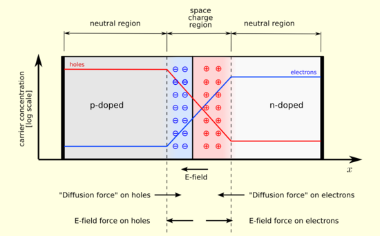 Figure A. A p–n junction in thermal equilibrium with zero bias voltage applied. Electrons and holes concentration are reported respectively with blue and red lines. Gray regions are charge neutral. Light red zone is positively charged. Light blue zone is negatively charged. The electric field is shown on the bottom, the electrostatic force on electrons and holes and the direction in which the diffusion tends to move electrons and holes.
The electric field created by the space charge region opposes the diffusion process for both electrons and holes. There are two concurrent phenomena: the diffusion process that tends to generate more space charge, and the electric field generated by the space charge that tends to counteract the diffusion. The carrier concentration profile at equilibrium is shown in figure A with blue and red lines. Also shown are the two counterbalancing phenomena that establish equilibrium.
 Figure B. A p–n junction in thermal equilibrium with zero bias voltage applied. Under the junction, plots for the charge density, the electric field and the voltage are reported.
The space charge region is a zone with a net charge provided by the fixed ions (donors or acceptors) that have been left uncovered by majority carrier diffusion. When equilibrium is reached, the charge density is approximated by the displayed step function. In fact, the region is completely depleted of majority carriers (leaving a charge density equal to the net doping level), and the edge between the space charge region and the neutral region is quite sharp (see figure B, Q(x) graph). The space charge region has the same magnitude of charge on both sides of the p–n interfaces, thus it extends farther on the less doped side (the n side in figures A and B).
Forward bias
In forward bias, the p-type is connected with the positive terminal and the n-type is connected with the negative terminal.
 PN junction operation in forward bias mode showing reducing depletion width. Both p and n junctions are doped at a 1e15/cm3 doping level, leading to built-in potential of ~0.59V. Reducing depletion width can be inferred from the shrinking charge profile, as fewer dopants are exposed with increasing forward bias.
With a battery connected this way, the holes in the P-type region and the electrons in the N-type region are pushed towards the junction. This reduces the width of the depletion zone. The positive charge applied to the P-type material repels the holes, while the negative charge applied to the N-type material repels the electrons. As electrons and holes are pushed towards the junction, the distance between them decreases. This lowers the barrier in potential. With increasing forward-bias voltage, the depletion zone eventually becomes thin enough that the zone's electric field can't counteract charge carrier motion across the p–n junction, consequently reducing electrical resistance. The electrons which cross the p–n junction into the P-type material (or holes which cross into the N-type material) will diffuse in the near-neutral region. Therefore, the amount of minority diffusion in the near-neutral zones determines the amount of current that may flow through the diode.
Only majority carriers (electrons in N-type material or holes in P-type) can flow through a semiconductor for a macroscopic length. With this in mind, consider the flow of electrons across the junction. The forward bias causes a force on the electrons pushing them from the N side toward the P side. With forward bias, the depletion region is narrow enough that electrons can cross the junction and inject into the P-type material. However, they do not continue to flow through the P-type material indefinitely, because it is energetically favorable for them to recombine with holes. The average length an electron travels through the P-type material before recombining is called the diffusion length, and it is typically on the order of microns.[2]
Although the electrons penetrate only a short distance into the P-type material, the electric current continues uninterrupted, because holes (the majority carriers) begin to flow in the opposite direction. The total current (the sum of the electron and hole currents) is constant in space, because any variation would cause charge buildup over time (this is Kirchhoff's current law). The flow of holes from the P-type region into the N-type region is exactly analogous to the flow of electrons from N to P (electrons and holes swap roles and the signs of all currents and voltages are reversed).
Therefore, the macroscopic picture of the current flow through the diode involves electrons flowing through the N-type region toward the junction, holes flowing through the P-type region in the opposite direction toward the junction, and the two species of carriers constantly recombining in the vicinity of the junction. The electrons and holes travel in opposite directions, but they also have opposite charges, so the overall current is in the same direction on both sides of the diode, as required.
The Shockley diode equation models the forward-bias operational characteristics of a p–n junction outside the avalanche (reverse-biased conducting) region.
Reverse bias
 A silicon p–n junction in reverse bias.
Reverse biased usually refers to how a diode is used in a circuit. If a diode is reverse biased, the voltage at the cathode is higher than that at the anode. Therefore, no current will flow until the diode breaks down. Connecting the P-type region to the negative terminal of the battery and the N-type region to the positive terminal corresponds to reverse bias. The connections are illustrated in the following diagram:
Because the p-type material is now connected to the negative terminal of the power supply, the 'holes' in the P-type material are pulled away from the junction, causing the width of the depletion zone to increase. Similarly, because the N-type region is connected to the positive terminal, the electrons will also be pulled away from the junction. Therefore the depletion region widens, and does so increasingly with increasing reverse-bias voltage. This increases the voltage barrier causing a high resistance to the flow of charge carriers thus allowing minimal electric current to cross the p–n junction. The increase in resistance of the p–n junction results in the junction behaving as an insulator.
The strength of the depletion zone electric field increases as the reverse-bias voltage increases. Once the electric field intensity increases beyond a critical level, the p–n junction depletion zone breaks-down and current begins to flow, usually by either the Zener or avalanche breakdown processes. Both of these breakdown processes are non-destructive and are reversible, so long as the amount of current flowing does not reach levels that cause the semiconductor material to overheat and cause thermal damage.
This effect is used to one's advantage in zener diode regulator circuits. Zener diodes have a certain - low - breakdown voltage. A standard value for breakdown voltage is for instance 5.6V. This means that the voltage at the cathode can never be more than 5.6V higher than the voltage at the anode, because the diode will break down - and therefore conduct - if the voltage gets any higher. This effectively regulates the voltage over the diode.
Another application where reverse biased diodes are used is in Varicap diodes. The width of the depletion zone of any diode changes with voltage applied. This varies the capacitance of the diode. For more information, refer to the Varicap article.
Electrostatics
For a p–n junction Poisson's equation becomes

where
 is the electric potential, ρ is the charge density,
  is permittivity and q is the magnitude of the electron charge.
Since the total charge on either side of the depletion region must cancel out it is

From the above equations and by deploying basic calculus it can be shown that the total width of the depletion region is

Furthermore, by implementing the Einstein relation and assuming the semiconductor is nondegenerate (i.e. the product p0n0 is independent of the Fermi energy) it follows that

where T is the temperature of the semiconductor and k is Boltzmann constant. [3]
Summary
The forward-bias and the reverse-bias properties of the p–n junction imply that it can be used as a diode. A p–n junction diode allows electric charges to flow in one direction, but not in the opposite direction; negative charges (electrons) can easily flow through the junction from n to p but not from p to n and the reverse is true for holes. When the p–n junction is forward biased, electric charge flows freely due to reduced resistance of the p–n junction. When the p–n junction is reverse biased, however, the junction barrier (and therefore resistance) becomes greater and charge flow is minimal.
Non-rectifying junctions
In the above diagrams, contact between the metal wires and the semiconductor material also creates metal-semiconductor junctions called Schottky diodes. In a simplified ideal situation a semiconductor diode would never function, since it would be composed of several diodes connected back-to-front in series. But in practice, surface impurities within the part of the semiconductor which touches the metal terminals will greatly reduce the width of those depletion layers to such an extent that the metal-semiconductor junctions do not act as diodes. These "nonrectifying junctions" behave as ohmic contacts regardless of applied voltage polarity.
See also
- Diode and junction diode
- Diode modelling
- Semiconductor
- Transistor
- Field effect transistor
- Bipolar junction transistor
- Alloy-junction transistor
- p-n-p transistor
- n-p-n transistor
- Transistor-transistor logic
- Capacitance voltage profiling
- Deep-level transient spectroscopy
- Solar cell
- Semiconductor detector
References
- ^ an account of Ohl's discovery is in Riordan, Michael; Lillian Hoddeson (1988). Crystal fire: the invention of the transistor and the birth of the information age. USA: W. W. Norton & Company. pp. 88–97. ISBN 0393318516. http://books.google.com/books?id=SZ6wm5ZSUmsC&pg=PA92.
- ^ Hook, J. R.; H. E. Hall (2001). Solid State Physics. John Wiley & Sons. ISBN 0-471-92805-4.
- ^ Handbook Of Photovoltaic Science And Engineering by Antonio Luque & Steven Hegedus, Wiley 2003
- Olav Torheim, Elementary Physics of P-N Junctions, 2007.
- 'Solid state devices' by Millman and Halkias
Junctions
- Back junction is a solar cell featuring the formation of a p-n junction at its rear surface
- Single-junction
- Heterojunction
- Multijunction
- P-i-n and n-i-p
External links
- PN Junction Properties Calculator
- PN Junction Lab free to use on nanoHUB.org allows simulation and study of a P-N junction diode with different doping and materials. Users can calculate current-voltage (I-V) & capacitance-voltage (C-V) outputs, as well.
- Theory of P-N Diodes - Dr. Vasileska (2009)
Categories:- Semiconductor structures


Wikimedia Foundation. 2010.