- GeForce 400 Series
-
Nvidia GeForce 400 Series 
Codename(s) GF100 / GF104 / GF106 / GF108 (Fermi) Release date April 12, 2010 Entry-level GPU GT 430, GT 440 Mid-range GPU GTS 450 High-end GPU GTX 460, GTX 465, GTX 470, GTX 480 Direct3D and shader version Direct3D 11
Shader Model 5.0OpenGL version OpenGL 4.2 OpenCL version OpenCL 1.1 Predecessor GeForce 300 Series Successor GeForce 500 Series The GeForce 400 Series is the 11th generation of Nvidia's GeForce graphics processing units. The series was originally slated for production in November 2009,[1] but, after a number of delays, launched on March 26, 2010 with availability following in April 2010.
Contents
Overview
Nvidia has given the architecture an internal name of Fermi, after the Italian physicist Enrico Fermi, a key developer of the nuclear reactor, who also gave his name to the Fermi acceleration mechanism in astrophysics. Nvidia claims that the Fermi architecture is the next major step in its line of GPUs following the G80.
The GF100, the first Fermi-architecture product, is large: 512 stream processors, in sixteen groups of 32, and 3.0 billion transistors, manufactured by TSMC in a 40 nm process. It is Nvidia's first chip to support OpenGL 4.0 and Direct3D 11. At launch, no product was available with all the stream processors active: the GTX 480 has one group disabled, the GTX 470 has two groups and one memory controller disabled, and the GTX 465 has five groups and two memory controllers disabled. Consumer GeForce cards come with 256MB attached to each of the enabled GDDR5 memory controllers, for a total of 1.5, 1.25 or 1.0GB; the Tesla C2050 has 512MB on each of six controllers, and the Tesla C2070 has 1024MB per controller. Both the Tesla cards have fourteen active groups of stream processors.
In the more expensive "Tesla" configurations, the chip features optional ECC protection on the memory, and can perform one double-precision floating-point operation per cycle per core; the consumer GeForce cards are artificially driver restricted to one DP operation per four cycles. With these features, combined with support for Visual Studio and C++, Nvidia hopes to appeal to the High-Performance Computer users who might presently be using Tesla systems.[2]
History
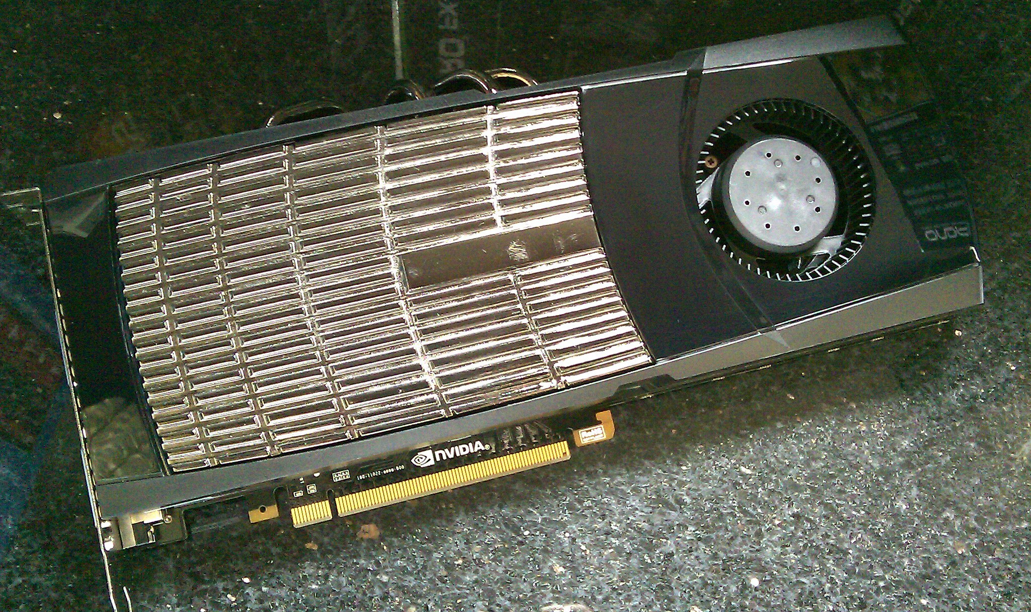
 NVIDIA GeForce GTX 480
 Fermi core chip on GTX 480 card
On 30 September 2009, Nvidia released a white paper describing the architecture:[3] the chip features 16 'Streaming Multiprocessors' each with 32 'CUDA Cores' capable of one single-precision operation per cycle or one double-precision operation every other cycle, a 40-bit virtual address space which allows the host's memory to be mapped into the chip's address space, meaning that there is only one kind of pointer and making C++ support significantly easier, and a 384-bit wide GDDR5 memory interface. As with the G80 and GT200, threads are scheduled in 'warps', sets of 32 threads each running on a single shader core. While the GT200 had 16 KB 'shared memory' associated with each shader cluster, and required data to be read through the texturing units if a cache was needed, GF100 has 64 KB of memory associated with each cluster, which can be used either as a 48 KB cache plus 16 KB of shared memory, or as a 16 KB cache plus 48 KB of shared memory, along with a 768 KB L2 cache shared by all 16 clusters.
The white paper describes the chip much more as a general purpose processor for workloads encompassing tens of thousands of threads - reminiscent of the Tera MTA architecture, though without that machine's support for very efficient random memory access - than as a graphics processor.
Pre-launch statements
At a press event on January 7, 2010 at CES Jen-Hsun Huang said that the GF100 products were in production but did not give a shipping date.[4]
On January 18, 2010, Nvidia released the GF100 graphics architecture details through a white paper.[5]
On February 2, 2010, Nvidia tweeted the official titles of the GF100 (Fermi) retail cards, the GeForce GTX 480 and the GeForce GTX 470.[6]
February 22, 2010: According to Nvidia's twitter update, the Fermi based Geforce GTX 400 series will be "unveiled" at the PAX East 2010,[7] in a later update Nvidia released the launch date of March 26, 2010 for the GTX 470 and GTX 480 to clear up confusion over the PAX announcement.[8]
March 4, 2010: Tom Petersen at NVIDIA describes how the performance of GeForce GTX 480 compares to the Radeon HD 5870 in a single test case.[9]
March 26, 2010: The complete architecture along with the GTX 470 and 480 were officially launched at PAX EAST.
April 7, 2010: Limited product availability started to show.[10][11]
April 12, 2010: Official release date for most manufacturers, bar EVGA, which released its cards on April 7, 2010.
Current limitations and trade-offs
The quantity of on-board SRAM per ALU actually decreased proportionally compared to the previous G200 generation, despite the increase of the L2 cache from 256kB per 240 ALUs to 768kB per 512 ALUs, since Fermi has only 32768 registers per 32 ALUs (vs. 16384 per 8 ALUs), only 48kB of shared memory per 32 ALUs (vs. 16kB per 8 ALUs), and only 16kB of cache per 32 ALUs (vs. 8kB constant cache per 8 ALUs + 24kB texture cache per 24 ALUs). Parameters such as the number of registers can be found in the CUDA Compute Capability Comparison Table in the reference manual.[12]
Products
- 1 SPs - Shader Processors - Unified Shaders (Vertex shader / Geometry shader / Pixel shader) : TMUs - Texture mapping units : Render Output unit
- 2 Each Streaming Multiprocessor(SM) in the GPU of GF100 architecture contains 32 SPs and 4 SFUs. Each Streaming Multiprocessor(SM) in the GPU of GF104/106/108 architecture contains 48 SPs and 8 SFUs. Each SP can fulfil one single precision fused multiply–add (FMA) operation per cycle. Each SFU can fulfil four SF operations per cycle. One FMA operation counts for two floating point operations. So the theoretical single precision peak performance, with shader count [n] and shader frequency [f, GHz], can be estimated by the following, FLOPSsp ≈ f × n × 2 (FMA). Total Processing Power: for GF100 FLOPSsp ≈ f × m ×(32 SPs × 2(FMA) + 4 × 4 SFUs) and for GF104/106/108 FLOPSsp ≈ f × m × (48 SPs × 2(FMA) + 4 × 8 SFUs) or for GF100 FLOPSsp ≈ f × n × 2.5 and for GF104/106/108 FLOPSsp ≈ f × n × 8 / 3.[13]
SP - Shader Processor (Unified Shader, CUDA Core), SFU - Special Function Unit, SM - Streaming Multiprocessor.
- 3 Each SM in the GF100 contains 4 texture filtering units for every texture address unit. The complete GF100 die contains 64 texture address units and 256 texture filtering units[14] Each SM in the GF104/106/108 architecture contains 8 texture filtering units for every texture address unit. The complete GF104 die contains 64 texture address units and 512 texture filtering units, the complete GF106 die contains 32 texture address units and 256 texture filtering units and the complete GF108 die contains 16 texture address units and 128 texture filtering units.[15]
Model Year Code name Fab (nm) Transistors (million) Die size (mm2) Die Count Bus interface Memory (MiB) SM count Config core 1,3 Clock rate Fillrate Memory configuration API support (version) GFLOPs (FMA)2 TDP (watts) Release price (USD) Core (MHz) Shader (MHz) Memory (MHz) Pixel (GP/s) Texture (GT/s) Bandwidth (GB/s) DRAM type Bus width (bit) DirectX OpenGL OpenCL GeForce 405 (OEM) September 16, 2011 ? 40 ? ? 1 PCIe 2.0 x16 512
10241 ? 790 1402 1580 ? ? 12.6 GDDR3 64 11 4.2 1.1 ? 25 OEM GeForce GT 420 (OEM) September 3, 2010 GF108 40 585 116 1 PCIe 2.0 x16 2048 1 48:8:4 700 1400 1800 2.8 5.6 28.8 GDDR3 128 11 4.2 1.1 134.4 50 OEM GeForce GT 430 (OEM) October 11, 2010 GF108 40 585 116 1 PCIe 2.0 x16 2048 2 96:16:4 700 1400 1600
18002.8 11.2 25.6
28.8GDDR3 128 11 4.2 1.1 268.8 60 OEM GeForce GT 430 October 11, 2010 GF108 40 585 116 1 PCIe 2.0 x16 1024 2 96:16:4 700 1400 1800 2.8 11.2 28.8 GDDR3 128 11 4.2 1.1 268.8 49 $79 GeForce GT 440 February 1, 2011 GF108 40 585 116 1 PCIe 2.0 x16 512
1024
20482 96:16:4 810 1620 1800
32003.24 12.96 28.8
51.2GDDR3
GDDR5128 11 4.2 1.1 311.04 65 $79 GeForce GT 440 (OEM) October 11, 2010 GF106 40 1170 238 1 PCIe 2.0 x16 1536
30723 144:24:24 594 1189 1800 14.26 14.26 43.2 GDDR3 192 11 4.2 1.1 342.43 56 OEM GeForce GTS 450 (OEM) October 11, 2010 GF106 40 1170 238 1 PCIe 2.0 x16 1536 3 144:24:24 790 1580 1804 18.96 18.96 86 GDDR5 192 11 4.2 1.1 455.04 106 OEM GeForce GTS 450 September 13, 2010 GF106 40 1170 238 1 PCIe 2.0 x16 512
10244 192:32:16 783 1566 1804 12.53 25.06 57.73 GDDR5 128 11 4.2 1.1 601.34 106 $129 GeForce GTX 460 SE November 15, 2010 GF104 40 1950 332 1 PCIe 2.0 x16 1024 6 288:48:32 650 1300 1700 20.8 31.2 108.8 GDDR5 256 11 4.2 1.1 748.8 150 $160?-$180? GeForce GTX 460 (OEM) October 11, 2010 GF104 40 1950 332 1 PCIe 2.0 x16 1024 7 336:56:32 650 1300 3400 20.8 36.4 108.8 GDDR5 256 11 4.2 1.1 873.6 150 OEM GeForce GTX 460 July 12, 2010 GF104 40 1950 332 1 PCIe 2.0 x16 768 7 336:56:24 675 1350 3600 16.2 37.8 86.4 GDDR5 192 11 4.2 1.1 907.2 150 $199 1024 336:56:32 21.6 115.2 256 160 $229 GeForce GTX 465 May 31, 2010 GF100 40 3200 529 1 PCIe 2.0 x16 1024 11 352:44:32 607 1215 3206 19.42 26.71 102.6 GDDR5 256 11 4.2 1.1 855.36 200 $279 GeForce GTX 470 March 26, 2010 GF100 40 3200 529 1 PCIe 2.0 x16 1280 14 448:56:40 607 1215 3348 24.28 34 133.9 GDDR5 320 11 4.2 1.1 1088.64 215 $349 GeForce GTX 480 March 26, 2010 GF100 40 3200 529 1 PCIe 2.0 x16 1536 15 480:60:48 700 1401 3696 33.60 42 177.4 GDDR5 384 11 4.2 1.1 1344.96 250 $499 As of November 8, 2010, Nvidia released the GF110 chip, along with the GTX580 (480's replacement). It is a redesigned GF100 chip, which uses significantly less power. This allows Nvidia to enable all 16 SMs (all 16 cores), which was previously impossible on the GF100 "NVIDIA GeForce GTX 580". http://www.nvidia.com/object/product-geforce-gtx-580-us.html.. Various features of the GF100 architecture remain available only on the more expensive Tesla series of cards.[16] For consumer products, double precision performance has been limited to a quarter of that of the "full" Fermi architecture. Error checking and correcting memory (ECC) is also disabled on consumer cards.[17] The GF100 cards provide Compute Capability 2.0, while the GF104/106/108 cards provide Compute Capability 2.1.
Chipset table
Main article: Comparison of Nvidia graphics processing unitsSee also
- Comparison table of GeForce 400 Series
- GeForce 8 Series
- GeForce 9 Series
- GeForce 200 Series
- GeForce 300 Series
- GeForce 500 Series
- Nvidia Quadro
- Nvidia Tesla
References
- ^ "OFFICIAL: NVIDIA says GT300 on schedule for Q4 2009, yields are fine - Bright Side Of News*". Brightsideofnews.com. http://www.brightsideofnews.com/news/2009/9/25/nvidia-says-gt300-on-schedule-for-q4-20092c-yields-are-fine.aspx. Retrieved 2010-09-20.
- ^ "Next Generation CUDA Architecture, Code Named Fermi". Nvidia.com. http://www.nvidia.com/object/fermi_architecture.html. Retrieved 2010-09-20.
- ^ http://www.nvidia.com/content/PDF/fermi_white_papers/NVIDIA_Fermi_Compute_Architecture_Whitepaper.pdf
- ^ "Live from NVIDIA's CES press event". Engadget. 2010-01-07. http://www.engadget.com/2010/01/07/live-from-nvidias-ces-press-event/. Retrieved 2010-09-20.
- ^ "The next generation of NVIDIA GeForce GPU". Nvidia.com. http://www.nvidia.com/object/gf100.html. Retrieved 2010-09-20.
- ^ "Twitter / NVIDIA GeForce: Fun Fact of the Week: GeFo ...". http://twitter.com/NVIDIAGeForce/status/8523402386.
- ^ "Twitter / NVIDIA GeForce: The wait is almost over! T ...". http://twitter.com/NVIDIAGeForce/status/9483846060.
- ^ "Twitter / NVIDIA GeForce: Apologies for the confusion ...". http://twitter.com/NVIDIAGeForce/status/9503345711.
- ^ "YouTube / GTX 480 Unigine and 3D Vision Surround Demo (GF100)". http://www.youtube.com/watch?v=vpdPSZB8A8E.
- ^ "NVIDIA’s GeForce GTX 400 Series Shows Up "Early"". http://www.anandtech.com/show/3642/nvidias-geforce-gtx-400-series-shows-up-early.
- ^ "http://www.evga.com/forums/tm.aspx?m=284103". http://www.evga.com/forums/tm.aspx?m=284103.
- ^ Compute Capability Comparison Table in "Page 147-148, Appendix G.1, CUDA 3.1 official reference manual". http://developer.download.nvidia.com/compute/cuda/3_1/toolkit/docs/NVIDIA_CUDA_C_ProgrammingGuide_3.1.pdf.. Page 97 in Appendix A lists the older NVIDIA GPUs and shows all G200 series to be compute capability 1.3, while Fermi-based cards have compute capability 2.x (page 14, Section 2.5).
- ^ siliconmadness.com (2010). "Nvidia Announces Tesla 20 Series". http://www.siliconmadness.com/2009/11/nvidia-announces-tesla-20-series.html.
- ^ NVIDIA's GeForce GTX 480 and GTX 470: 6 Months Late, Was It Worth the Wait?
- ^ NVIDIA’s GeForce GTX 460: The $200 King
- ^ "Statement by NVIDIA on their General CUDA GPU Computing Discussion forum". http://forums.nvidia.com/index.php?showtopic=165055.
- ^ "NVIDIA Tesla C2xxx webpage". http://www.nvidia.com/object/product_tesla_C2050_C2070_us.html., note from the description one may infer that on Teslas, ECC may be switched on and off using 1/8 of existing on-board memory, unlike standard ECC memory modules which requires 1/8 extra memory chips (that is, one extra chip to be mounted on the printed circuit board for every 8).
External links
- The Next Generation of Nvidia GeForce
- Fermi architecture
- GTX 400 Overview
- GeForce GTX 480
- GeForce GTX 470
- GeForce GTX 465
- GeForce GTX 460
- GeForce GTS 450
- GeForce GT 440
- GeForce GT 430
- GeForce GTX 485M
- GeForce GTX 480M
- GeForce GTX 470M
- GeForce GTX 460M
- GeForce GT 445M
- GeForce GT 435M
- GeForce GT 425M
- GeForce GT 420M
- GeForce GT 415M
- GeForce 410M
- GeForce 405
- Nvidia Parallel Nsight
- David Kanter (September 30, 2009). "Inside Fermi: Nvidia's HPC Push". realworldtech.com. http://www.realworldtech.com/page.cfm?ArticleID=RWT093009110932. Retrieved December 16, 2010.
Nvidia Graphics processing units Early chipsetsRIVA seriesGeForce 256 · GeForce 2 · GeForce 3 · GeForce 4 · GeForce 5 · GeForce 6 · GeForce 7 · GeForce 8 · GeForce 9 · GeForce 100 · GeForce 200 · GeForce 300 · GeForce 400 · GeForce 500Other seriesTechnologiesMotherboard chipsets GeForce SeriesnForce SeriesnForce 220/415/420 · nForce2 · nForce3 · nForce4 · nForce 500 · nForce 600 · nForce 700 · nForce 900TechnologiesOther products Project DenverBridge chipsHandheldSoftwareAcquisitionsKey people Jen-Hsun Huang · Chris Malachowsky · Curtis Priem · David Kirk · Debora Shoquist · Dr. Ranga Jayaraman · Jonah M. AlbenCategories:- 2010 introductions
- Nvidia
- Video cards

Wikimedia Foundation. 2010.