- Photonic metamaterial
-
Electromagnetism 
Electricity · Magnetism Lorentz force law · emf · Electromagnetic induction · Faraday’s law · Lenz's law · Displacement current · Maxwell's equations · EM field · Electromagnetic radiation · Liénard–Wiechert potential · Maxwell tensor · Eddy currentPhotonic metamaterials, also known as Optical metamaterials, are a type of electromagnetic metamaterial, which are designed to interact with optical frequencies which are terahertz (THz), infrared (IR), and eventually, visible wavelengths. As a type of metamaterial, the periodic structures are made up of single units called cells. These single units are much smaller than the wavelength of the radiated source. With photonic metamaterials the radiated source is at optical wavelengths. Furthermore, the subwavelength period distinguishes the photonic metamaterial from photonic band gap or photonic crystal structures. This is because the special optical properties do not arise from photonic bandgaps, but rather from a subwavelength interaction with the light spectrum, which mimics atoms or ions. However, the periodic cells (meta-atoms) are fabricated on a scale that is magnitudes larger than the atom, yet smaller than the radiated wavelength.[1][2]
Electromagnetic metamaterials in general are designed to operate at different frequencies. For example, prior and current research is in the microwave domain with physical periodic cell structures on the scale of millimeters. Because the optical wavelengths (wavelengths of a few micrometres) are much shorter than microwave frequencies, photonic metamaterial cell structures are on the scale of nanometers.[1][2][3]
In a naturally occurring, (conventional) material, the response to electric and magnetic fields, and hence to light, is determined by the atoms[4][5] As a type of metamaterial, the photonic metamaterial is an artificially engineered structure. Therefore, each periodic cell is designed with specific parameters by which it interacts with the radiated field at optical frequencies. At the same time, however, metamaterials in general, which includes photonic metamaterials, are described as homogeneous materials, or in other words, utilizing an effective medium model.[1][2][4]
Furthermore, demonstrating artificial magnetism at high frequencies, resulting in strong magnetic coupling, is contrasted with the usual or normal weak magnetic coupling of ordinary materials. This can then be applied to achieving negative index of refraction in the optical range, and developing approaches that show potential for application to optical cloaking. In addition, photonic metamaterials are an emergent tool in transformation optics.[6]
Finally, regarding photonic crystals, the size and periodicity of the scattering elements are on the order of the wavelength rather than subwavelength. A photonic crystal cannot be described as a homogeneous medium so it is not possible to define values of ε or u. However, photonic crystal materials are typically composed of insulators and therefore can exhibit very low losses, even at optical frequencies.[7]
The development of photonic metamaterials
 A comparison of refraction in a left-handed metamaterial to that in a normal material
Artificial composite structures – metamaterials
In tandem with the assemblage of the first metamaterials, came the awareness of possibilities that were once thought not possible before the mid-1990s such as Nanometer-scale imaging, an opposite refraction phenomenon, and cloaking objects . These observable, scientific phenomena are possible because structural units of the metamaterials can be tailored in shape, size, and spacing. Their composition, and their form or structure, can be finely adjusted. Inclusions are specifically designed, and then placed at desired locations. Each design alteration, and - or change-up in spacing, creates a new variation in the function of a metamaterial.[8] As of 2009 these possibilities are occurring in the lab,[3] and some related metamaterial technologies are already in the commercial sector.[9][10]
A basis for understanding metamaterials in general is the propagation of light in conventional optical materials, such as glass or prisms. Although light consists of an electric field and a magnetic field, ordinary optical materials have a vigorous interaction only with the electric field. In comparison, the corresponding faint, magnetic interaction is essentially nil. This results in only the most common optics effects. These common optical effects include ordinary refraction with common diffraction limitations in lenses and imaging. In other words, this property limits the ability to control electromagnetic waves, which includes visible light, propagating through these materials. While researching whether or not matter interacts with the magnetic component of light, Victor Veselago (1967) envisioned the possibility of extraordinary refraction, occurring with a negative sign according to Maxwell's equations. According to Veselago, and confirmed by researchers 30 years later, a refractive index with a negative sign is the result of permittivity, ε < 0 (less than zero) and magnetic permeability, μ < 0 (also less than zero).[3][8][11]
Negative permeability and negative refractive index
See also: History of metamaterials Photograph of the metamaterial lattice used to demonstrate negative refraction. The array of square split-ring resonators gives the material a negative magnetic permeability, whereas the array of straight wires gives it a negative permittivity
Natural materials, such as precious metals, can achieve permittivity values of less than zero (ε < 0) up to the visible frequencies. However, at terahertz, infrared, and visible frequencies (optical range), natural materials have a very weak magnetic coupling component, or permeability. In other words, suceptibility to the magnetic component of the radiated light, or electromagnetic wave, can be considered negligible. Nevertheless, producing negative values for permeability (μ < 0) is necessary to produce the negative refractive index of the photonic metamaterial.[8]
Thirty years after Victor Veselago's analytical paper, an artificial negative value for permeability was achieved with the first repeating split-ring resonator (SRR) structure. The SRR achieved negative permeability (μ < 0) within a narrow range of frequency. This was then combined with a symmetrically positioned electric conducting post, which created the first actual left-handed material LHM - a type of Metamaterial- operating in the microwave sector. A similarly structured left-handed material, with ehanced capabilities compared to the first, soon followed. This also was demonstrated at microwave frequencies. Although experiments and simulations on these left handed materials demonstrated the presence of a left-handed propagation band, the first experimental confirmation of negative index of refraction occurred at a time shortly after the above, and once again at microwave frequencies.[3][12][13]
The negative index metamaterial is a material, which behaves contrary to the conventional "right-handed" interaction of light found in conventional optical materials. Hence, these are dubbed left-handed materials or negative index materials (NIMs), among other nomenclatures. Simply put, metamaterials, LHMs - or NIMs - have effectively expanded the material response.[3][12][13]
To date (March 2010), only artificially fabricated LHMs have the distinction of exhibiting this capability; even when compared to photonic crystals. Photonic crystals, like many other known systems, can exhibit unusual propagation behavior such as reversal of phase and group velocities. But, negative refraction does not occur in these systems, and not yet realistically in Photonic crystals.[12][14][15]
Naturally occurring ferromagnetic and antiferromagnetic materials can achieve magnetic resonance, but with significant losses. Furthermore, characteristic of natural materials such as natural magnets, and ferrites, resonance for the electric (coupling) response and magnetic (coupling) response do not occur simultaneously, at the same frequencies. These constraints imply that Veselago’s theoretical analysis of a material with extraordinary properties might have remained in the background as an intriguing curiosity. However, explorations into the possibility of manufacturing materials which have the enlarged electric and magnetic response began in the mid-1990s. Although earlier research into artificial materials dates back to the 1940s, and even the late 19th century, advances of the 1990s in fabrication and the computational sciences led to a resurgence in research for these unconventional materials. Furthermore, Victor Veselago's seminal analysis has been cited in over 1500 peered reviewed articles, including a number of books on the subject of artificial materials that have a negative index, and variations thereof.[11][16][17][18]
Optical frequency metamaterials
Within a only a few years the structures were scaled down for optical frquencies with nano-scale metamaterials. Photonic metamaterial SRRs have now reached scales below 100 nanometers, with special electron beam and nanolithography techniques. One type of nanoscale SRR cell has three very small metallic rods which are physically connected. This is configured into a U type of a shape, which then functions as a nano-inductor. The gap between the tips of the U-shape function as a nano-capacitor. Hence, it is then a nano-LC resonator, with resonance occurring at optical frequencies. These are the actual "inclusions" mentioned in the metamaterial literature, which create local electric and magnetic fields when externally excited. A notable characteristic occurs at optical frequencies; these inclusions are usually ten times smaller than the vacuum wavelength of the light c0, at resonance frequency. The fabrication of the inclusions in this way can then be evaluated by using an effective medium approximation.[3][11]
Finally, photonic metamaterials open up a way to overcome the constraints (stated above) set by ordinary materials. The proper design of the inclusions (meta-atoms), which are elementary building blocks, now allow for a magnetic response with sufficient magnitude at optical frequencies. This includes negative permeability, μ < 0, despite the fact that these are constructed from non-magnetic materials. Furthermore, analogous to ordinary optical material, such a photonic metamaterial can be treated as an effective medium that is characterized by effective medium parameters ε(ω) and μ(ω), or similarly, εeff and μeff.[11][19]
Effective medium model
An effective (transmission) medium approximation means that the combined overall effect of the inclusions, when reacting to an external excitation, is approximated to evaluate the metamaterial slab (the medium) as "effectively" homogeneous. The slab also has effective parameters, which include effective ε and µ. These are also approximated over the entire medium. Separate inclusions may have different values, but the overall effect results in an approximated effect for each parameter, hence, effective ε, effective µ.[20]
Among other properties, metamaterials can be described in terms of macroscopic quantities: permittivity, permeability, and index of refraction.
Metamaterials are most often intentionally fabricated as composite structures. These contain numerous elements that are identical in size, shape, capability, and electromagnetic parameters. These elements are engineered to be smaller than the propagating electromagnetic waves. Each element can be purposely designed to have a unique or similar value relative to the other components. However, due to the subwavelength structure of the elements, the entire composite material can be viewed and measured as homogeneous and isotropic. This then gives approximated electromagnetic values for the composite structure. These approximated values are effective permittivity, effective permeability, and an effective index of refraction. In other words, metamaterials from the microwave domain, into the infrared and optical ranges can be described in terms of macroscopic properties - rather than the varying values of each individual element. Hence, metamaterials can be constructed to exhibit properties not available in nature.[20]
Furthermore, although these materials are artificially constructed they are behaving as "real" materials, because real materials also have a periodic structure, but at atomic scales. Real materials have a refractive index, just like these artificial materials. However, these artificial materials are able to create the overall effect of negative refractive index. So there is no qualitative difference between a metamaterial and a natural dielectric material. There is only a quantitative difference - the unit sizes interacting with light (EM radiation) are magnitudes larger with left-handed metamaterials.[21]
The mechanics of optical frequency metamaterials
Stacking layers is important to achieve the desired results at optical frequencies. However, the surface configuration (non-planar, bulk) of the SRR metamaterial layers normally prevents stacking. Although a single-layer SRR structure can easily be constructed on a dielectric surface, it is relatively difficult to stack these bulk structures due to the tight alignment tolerance requirements.[3] However, a layer by layer stacking technique for SRRs was published in 2007. It uses dielectric spacers to apply a planarization procedure to flatten the SRR layer.[22] As a result it appears that any number of layers can be made this way, including any chosen number of unit cells as well as intentional designing of the spatial arrangements of subsequent layers.[3][22]
Photonic metamaterials: coupling magnetism at optical frequencies
To be characterized as a left-handed material there is a requirement for negative magnetic permeability μ. This was originally achieved in a left-handed medium (metamaterial) at microwave frequencies by using arrays of split-ring resonators, to demonstrate experimental verification of a negative index of refraction.[23] In most natural occurring materials, the magnetically coupled response starts to taper off at frequencies in the gigahertz range, which also means significant magnetism does not occur at optical frequencies. This creates a state where the effective permeability of the material is unity, μeff = 1. Hence, the magnetic component of a radiated electromagnetic field has virtually no effect on natural occurring materials at optical frequencies.[24]
As metamaterials evolve, a new domain of optical materials has been developed, and magnetic permeability μeff no longer equals unity for materials at optical frequencies. For metamaterials μeff ≠ 1, and much research and experimentation has been accomplished for permeability less than 0 (negative values); μeff < 0.[5]
Reviewing the characteristics of predetermined, engineered, periodic structures such as SRRs leads to an understanding of the physics of a periodic metamaterial. Meta-atoms are used to create conditions where a normally weak magnetic effect on materials is now strengthened in the new artificial materials. A meta-atom could be an SRR cell, the arrayed wire component of a YIG tuner, or any other artificial material designed to be periodic, and responsive at a fraction of the radiated wavelength.[5]
In such a design, the meta-atom becomes a larger scale, millimeter or nanometer-sized-magnetic dipole, when compared to the picometer sized atom. A meta-atom creates a magnetic dipole moment analogous to the magnetic dipole moment of natural atoms. For meta-atom constructed from the precious metal, gold the condition of μ < 0 can be achieved at telecommunication frequencies but, still not across the range of the visible frequencies. The visible frequency has been elusive because the plasma frequency of any metal is the ultimate limiting condition.[5]
Researchers are earnestly engaged in combining negative "magnetic" permeability μ < 0 with negative "electric" permittivity ε < 0, which can occur in each meta-atom when engineered to do so.
In 2006, researchers from various groups agreed to state the following: "Possibly, the real potential of the photonic metamaterials lies in other unexplored areas, for example, in chiral metamaterials or in nonlinear metamaterials. In any case, given today’s possibilities regarding the nanofabrication of tailored “atoms,” only our own imagination and creativity set the limits."[5]
Proposal for metamaterials with optical frequencies response
By employing a combination of plasmonic and non-plasmonic nanoparticles, lumped circuit element nanocircuits at infrared and optical frequencies appear to be possible. Designing subwavelength lumped circuit element structures at infrared and optical frequencies has special challenges when compared to lower frequency domains. Conventional lumped circuit elements are not available in a conventional way.[25]
The concept and implementation of lumped circuit elements in the microwave and radio frequency (RF) domain for metamaterial design has proved to be effective. These are subwavelength structures. The lumped element concept has allowed for element simplification and circuit modularization. A similar concept applicable to materials that respond at terahertz (THz), infrared (IR), and visible wavelengths can be employed. However these lumped circuit elements must also be smaller than terahertz (THz), infrared (IR), and visible wavelengths. Nanoscale fabrication techniques do exist to accomplish this. Therefore, size reduction as an obstacle, may in time, be overcome.[25]
The response of metals at smaller wavelegnths is, however, a more pronounced limitation. Metals such as gold, silver, aluminum, and copper easily conduct currents at RF and microwave frequencies. Hence, these have been more easily integrated as materials employed in these regimes. At optical frequencies characteristics of some noble metals are altered. Rather than normal current flow, plasmonic resonances occur as the real part of the complex permittivity of these metals become negative. Therefore, the main current flow is actually the electric displacement current density ∂D / ∂t, and can be termed as the “flowing optical current". Solving this problem, then, becomes more than scaling down the element size.[25]
Being smaller than the wavelength, the impedance of the particle becomes dependent several factors. The particle's shape, size, material, along with the optical frequency illumination all contribute to determine the nanoparticle's impedance. The particle's orientation with the optical electric field may also help determine the impedance. The choice of material actually results in the type of impedance the nanoparticle will exhibit. If the material is a conventional silicon dielectric, with real permittivity εreal > 0 at optical frequencies, the nanoparticle will act as a capacitive impedance or, in other words - nanocapacitor. Conversely, if the material is a noble metal such as gold (Au) or silver (Ag), with a real permittivity less than zero, εreal < 0, then it takes on inductive characteristics. Hence, it becomes a nanoinductor. Finally, material loss is represented as a nano-resistor.[25][26]
Fabrication techniques
Because microwaves are much longer than terahertz and infrared wavelengths, photonic metamaterials are more difficult to realize. Metamaterials in the microwave domain can be fabricated from circuit board materials. In contrast lithography techniques must be employed to produce the rudimentary elements, nano-resonators, that can create photonic metamaterials. The earlier type of nano-resonators were based on the split-ring resonator in the microwave domain. These can be considered as simplified LC circuits. Inductance is achieved because the ring is split, and capacitance occurs across the gap.
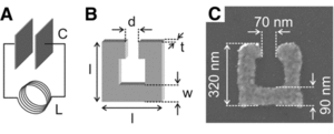 Illustration of the analogy between a conventional LC circuit (A), consisting of an inductance L, a capacitance C, and the single SRRs used here (B). l, length; w, width; d, gap width; t, thickness. (C) An electron micrograph of a typical SRR fabricated by electron beam lithography.
Other types of subwavelength photonic materials soon followed. In one instance, a periodic arrangement of short wires, and in another instance metallic pieces with varied shapes successfully interact at shorter wavelengths. In a different study, rather than the isolated nano-resonator structure, the whole metamaterial can be electrically connected for desired photonic subwavelength result.
In the following sections, some of the fabrication techniques are discussed.
Electron beam lithography
Because state-of-the-art photolithography is limited by the diffraction limit, electron beam lithography (EBL) shows an advantage. The unit sizes that make up the photonic metamaterial are beyond the resolution limit of photolithography. Instead, EBL is usually employed at this frequency range to construct a single layer of metamaterial atop a transparent substrate (2 dimensional). With nanometer beamwidths, EBL generates chosen patterns on the surface of materials at nanoscale resolution. Practical first and second generation structures were constructed with this technique, and experimentally demonstrated. The second generation showed improvement. There are still limitations using this writing technique including the high cost of fabrication. Furthermore, only small areas can be fabricated within a reasonable time and at acceptable cost.[19]
Focused ion beam nanostructuring
 Gas assisted deposition process
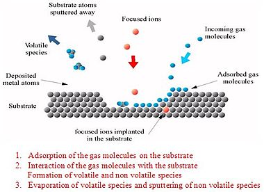 Gas assisted FIB etching process
Focused ion beam nanostructuring is a convenient tool for rapid prototyping of photonic metamaterials. The FIB is used as a micro-machining tool, to modify or machine materials at the micro- and nanoscale. FIB micro machining has become a broad field of its own, but nano machining with FIB is a field that still needs developing. The common smallest beam size is around 2.5 to 2.6 nanometers.[27]
Ions are positive, large, heavy and slow, whereas electrons (electron beam lithography) are negative, small, light and fast. The most important consequence of these properties is that ion beams will remove atoms from the substrate and because the beam position, dwell time, and size are so well controlled it can be applied to remove material locally in a highly controlled manner, down to the nanometer scale.[28]
Moreover, unlike an electron microscope, FIB is inherently destructive to the specimen. When the high-energy gallium ions strike the sample, they will sputter atoms from the surface. Gallium atoms will also be implanted into the top few nanometers of the surface, and the surface will be made amorphous.[27]
FIB tools are designed to etch or machine surfaces, an ideal FIB might machine away one atom layer without any disruption of the atoms in the next layer, or any residual disruptions above the surface. Yet currently because of the sputter the machining typically roughens surfaces at the submicrometre length scales.[29][30]
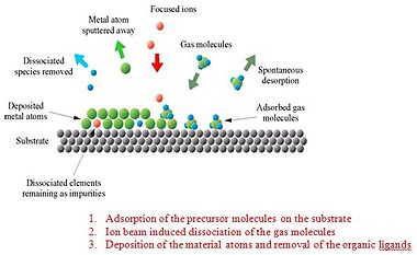
An FIB can also be used to deposit material via ion beam induced deposition. FIB-assisted chemical vapor deposition occurs when a gas, such as tungsten hexacarbonyl (W(CO)6) is introduced to the vacuum chamber and allowed to chemisorb onto the sample. By scanning an area with the beam, the precursor gas will be decomposed into volatile and non-volatile components; the non-volatile component, such as tungsten, remains on the surface as a deposition. This is useful, as the deposited metal can be used as a sacrificial layer, to protect the underlying sample from the destructive sputtering of the beam. From nanometers to hundred of micrometers in length, tungsten metal deposition allows to put metal lines right where needed. Other materials such as platinum, cobalt, carbon, gold, etc., can also be locally deposited.[27][29][30] Gas assisted deposition and FIB etching processes are shown to the right.[11][31]
Interference lithography
Interference lithography is comparatively inexpensive and is versatile.[11]
Tunable metamaterials at optical frequencies
Photonic metamaterials have become part of the pantheon of tunable and non-linear metamaterials. These are discussed in the Tunable metamaterials and Nonlinear metamaterials articles. However, a brief overview is given in this section.
As discussed throughout the article, some photonic applications are the purview of nanostructured metamaterials, which exhibit unique physical and optical properties. Areas of active research in optical materials are metamaterials that are capable of negative values for index of refraction (NIMs), and metamaterials that are capable of zero index of refraction (ZIMs). Complicated steps required to fabricate these nano-scale metamaterials have led to the desire for fabricated, tunable structures capable of the prescribed spectral ranges or resonances.
The most commonly applied scheme to achieve these effects is electro-optical tuning. Here the change in refractive index is proportional to either the applied electric field, or is proportional to the square modulus of the electric field. These are the Pockels effect and Kerr effect, respectively.
An alternative is to employ a nonlinear optical material as one of the constituents of this system, and depend on the optical field intensity to modify the refractive index, or magnetic parameters.[32]
Three-dimensional photonic metamaterials at optical frequencies
As has been already established, metamaterials are artificial media, and the unit cell of metamaterials is much smaller than the wavelength of light. As of December 2007, the physical characteristics of metamaterials, which include negative permeability and negative refraction, had been limited to demonstrations in two-dimensions. However, a group of researchers at the Physikalisches Institut - Universität Stuttgart perceived that the practical applications of these physical characteristics require three-dimensional bulk like structures. Up to this time, fabrication techniques were most compatible in the GHz range for microwave applications.[22]
By simply stacking printed circuit boards applications were available at GHz frequencies in the microwave range. This fabrication technique of metal–dielectric stacks is successful in this frequency range. However, a stacking technique in the optical (infrared) domain encountered technical problems which limited the number of stacked layers. So, an alternative to the unsuccessful stacking attempt was presented. The selected alternative is the split-ring resonator (SRR) structure. The SRR structure is widely used, and has induced negative values for permeability, for certain frequency ranges. SRR have been used in metamaterials since the 2001 demonstration.[22]
The completed SRR metamaterial layers cannot be stacked, as it is not a flat (or planar) surface. This design prevents stacking. So, the SRR layers were flattened with dielectric spacers.[22]
Dyakonov surface waves in photonic metamaterials
An idea for a type of photonic metamaterial is derived from the birefringent properties of photonic crystals. By utilizing metamaterial anisotropy, resonance conditions at which Dyakonov surface waves exist is met.[33]
Suitable photonic metamaterial structures can support lossless surface waves of the form envisaged by Dyakonov. Surface waves are a special type of waves that are confined at the very boundary between two different media. By their very nature, surface waves are unique tools to explore the properties of material interfaces. This includes not only intrinsic properties but also extrinsic effects, thus making surface waves ideal tools for sensing physical, chemical, and biological agents. They feature genuine physical phenomena as well as prospects for far-reaching applications.[33]
Negative-index photonic metamaterial at 780 nm wavelength
Photonic metamaterials are tailored artificial optical materials composed of sub-wavelength metallic building blocks that can be viewed as nano-scale electronic circuits. These building blocks or “photonic atoms” are densely packed into an effective material such that the operation wavelength (gamma) is ideally much larger than the lattice constant a for the polarization configuration shown in the metamaterial can be viewed as composed of two sets of sub-circuits or “atoms”: A coil with inductance L in series with two capacitors with net capacitance C as an LC circuit, providing a magnetic resonance at the LC resonance frequency. Long metallic wires, acting like a diluted metal below the effective plasma frequency of the arrangement. Negative magnetic permeability and the negative electric permittivity are created, which leads to lead to a negative index of refraction. Silver was used as constituent material because it is known to introduce significantly lower losses than gold and other noble metals at visible frequencies.[34]
Optical negative-index metamaterials
Describing the recent progress (in 2006) made in creating nanostructured metamaterials with a negative index at optical wavelengths, and discusses some of the devices that could result from these new materials.[35]
Experimental demonstration of near-infrared NIMs
Received 7 March 2005 and published in September of that year was the first fabrication and experimental verification of a transversely structured metal-dielectric-metal multilayer exhibiting a negative refractive index around 2 μm. Both the amplitude and the phase of the transmission and reflection were measured experimentally, and are in good agreement with a rigorous coupled wave analysis.[36]
Three-dimensional optical metamaterial
Here is a 3D optical metamaterial having negative refractive index with a very high figure of merit of 3.5. This metamaterial is made of cascaded ‘fishnet’ structures, with a negative index existing over a broad spectral range. Moreover, it can readily be probed from free space, making it functional for optical devices. Constructed as a 21-layer fishnet structure with a unit cell parameters of a = 5.860 µm, b = 5.565 µm and c = 5.265 µm.[37]
Negative refraction at 813 nm and 772 nm
Wavelengths of 813 nm and 772 nm approach the red end of the visible spectrum. A double negative refraction occurs at 813 nm and single negative refraction occurs at 772 nm.[38]
Phase-engineered metamaterial structures and devices
Electromagnetic metamaterials are inherently dispersive: their constitutive parameters (permittivity and permeability) are functions of frequency or, equivalently, their dispersion relation is a nonlinear function of frequency.
Since the invention of the superheterodyne receiver by Edwin Armstrong in 1918 and, later, the development of harmonic signal generators, most radio communication systems have been narrow-band in nature. However, the explosion of needs for high data-rate wireless links is currently producing a paradigmatic shift of radio toward broadband and ultra-wideband spectrum operation. In this context, the unprecedented and tailorable dispersive properties of metamaterials may provide solutions to several new challenges. While the past decades have focused on magnitude engineering and filter design we predict that the forthcoming decades will experience major interest in phase engineering (where the term "phase engineering" is intended to represent both "dispersion and nonlinearity" engineering) along with phase-engineered devices. In this case, metamaterials are expected to play an important role.[39]
See also
- Negative index metamaterials
- History of metamaterials
- Metamaterial cloaking
- Photonic metamaterials
- Metamaterial
- Metamaterial antennas
- Nonlinear metamaterials
- Photonic crystal
- Seismic metamaterials
- Split-ring resonator
- Acoustic metamaterials
- Metamaterial absorber
- Plasmonic metamaterials
- Terahertz metamaterials
- Tunable metamaterials
- Transformation optics
- Theories of cloaking
-
-
-
- Academic journals
-
-
-
-
-
- Metamaterials books
-
-
- Metamaterials Handbook
- Metamaterials: Physics and Engineering Explorations
Metamaterials scientists
- Richard W. Ziolkowski
- John Pendry
- David R. Smith
- Nader Engheta
- Ulf Leonhardt
- Vladimir Shalaev
External links
- Effective metamaterial parameter extraction algorithm developed by Zsolt Szabo
- Optics and photonics: Physics enhancing our lives
- Metamaterial Publications from Metagroup Duke Uinversity - a list of all publications by D. R. Smith and co-researchers up to 2009.
- Metamaterial articles in the mainstream media. Page hosted by Duke U. Metagroup
- Google scholar List of Papers by JB Pendry
- Imperial College, Department of Physics, Condensed Matter Theory Group
- OPAL: A Computational Tool For Photonics
- Experimental Verification of Reversed Cherenkov Radiation...
- Oriented Assembly of Metamaterials Particle self-assembly suggested for assembly of metamaterials at optical wavelengths.
- Subpicosecond Optical Switching with a Negative Index Metamaterial
General references
- Shalaev, Vladimir M., et al. Negative Index of Refraction in Optical Metamaterials arXiv.org. 17 pages.
- Shalaev, Vladimir M., et al. Negative index of refraction in optical metamaterials Opt. Lett. Vol. 30. 2005-12-30. 3 pages
References
- ^ a b c "Photonic Metamaterials". Encyclopedia of Laser Physics and Technology. I & II. Wiley. 2008-18. pp. 1. http://www.rp-photonics.com/photonic_metamaterials.html. Retrieved 2009-10-01.
- ^ a b c Capolino, Filippo (2009-10). Applications of Metamaterials. Taylor & Francis. pp. 29–1, 25–14, 22–1. ISBN 9781420054231. http://books.google.com/?id=8M0IqvcsHisC&pg=PT640. Retrieved 2009-10-01.
- ^ a b c d e f g h Ozbay, Ekmel (2008-11-01). "The Magical World of Photonic Metamaterials" (Free PDF download). Optics and Photonics News 19 (11): 22–27. doi:10.1364/OPN.19.11.000022. http://www.pi4.uni-stuttgart.de/NeueSeite/images/ozbay.pdf. Retrieved 2009-12-07.
- ^ a b Pendry, John (2006). "Photonics: Metamaterials in the sunshine". Nature Materials 5 (8): 599–600. Bibcode 2006NatMa...5..599P. doi:10.1038/nmat1697. PMID 16880801. http://www.cmth.ph.ic.ac.uk/photonics/Newphotonics/pdf/NatMatv5p599_2006.pdf. Retrieved 2009-10-08.
- ^ a b c d e Linden, Stefan; Enkrich, Christian; Dolling, Gunnar; Klein, Matthias W.; Zhou, Jiangfeng; Koschny, Thomas; Soukoulis, Costas M.; Burger, Sven et al. (2006). "Photonic Metamaterials: Magnetism at Optical Frequencies". IEEE Journal of selected topics in quantum electronics 12 (6): 1097. doi:10.1109/JSTQE.2006.880600. http://dsl.nju.edu.cn/litao/res/%5BPhotonic%20metamaterials-%20Magnetism%20at%20optical%20frequencies-S.%20Linden%5D.pdf. Retrieved 2009-13-2009.
- ^ Vladimir M., Shalaev. "Metamaterials: A New Paradigm of Physics and Engineering" (Lecture date (Part 1): March 06, 2008). Optical Metamaterials Fundamentals and Applications by Wenshan Cai and Vladimir Shalaev. Springer (book publisher) (Book publication date: November 30, 2009. ISBN 978-1-4419-1150-6. http://nanohub.org/courses/metamaterials. Retrieved 2010-02-06.
- ^ Smith, David; Pendry, John B.; Wiltshire, M. C. K. (2004-08-06). "Metamaterials and Negative Refractive Index" (see page 791. Free PDF download. PDF supplies links to other related articles, on this topic. This article cited by 452.). Science 305 (5685): 788–792. Bibcode 2004Sci...305..788S. doi:10.1126/science.1096796. PMID 15297655. http://hexagon.physics.wisc.edu/teaching/2009s%20ph721%20electrodynamics/pendry%20negative%20index%20review%20science%202004.pdf. Retrieved 2010-01-13.
- ^ a b c Shalaev, Vladimir M (2007-01). "Optical negative-index metamaterials". Nature photonics 01 (1): 41. Bibcode 2007NaPho...1...41S. doi:10.1038/nphoton.2006.49. http://cobweb.ecn.purdue.edu/~shalaev/MURI/publications/Optical%20negative-index%20metamaterials.pdf. Retrieved 2009-11-20.
- ^ "NETGEAR Ships 'The Ultimate Networking Machine' for Gamers, Media Enthusiasts and Small Businesses" ("...eight ultra-sensitive, internal, metamaterial antennas..."). The New York Times. 2009-10-20. http://markets.on.nytimes.com/research/stocks/news/press_release.asp?docKey=600-200909010830PR_NEWS_USPR_____SF68348-25UDEBBTNP0TL3Q8NDL3A9RQ33&provider=PR%20Newswire&docDate=September%201%2C%202009&press_symbol=217857&scp=2&sq=metamaterial&st=cse. Retrieved 2009-10-20.
- ^ Hurst, Brian (2009-09-28). "RAYSPAN Ships 20 Millionth Metamaterial Antenna" (press release by Reuters). Reuters. pp. 1. http://www.reuters.com/article/pressRelease/idUS93483+28-Sep-2009+PRN20090928. Retrieved 2009-10-20.
- ^ a b c d e f Capolino, Filippo (2009-10) (Chapter title: - "Fabrication and Optical Characterization of Photonic Metamaterials"). Applications of Metamaterials. Taylor & Francis. pp. 29–1, chapter 29. ISBN 9781420054231. http://books.google.com/?id=8M0IqvcsHisC&pg=PT533&dq=terahertz+metamaterials&cd=1#v=onepage&q=terahertz%20metamaterials.access date:2009-12-31
- ^ a b c Pendry, J., “New electromagnetic materials emphasize the negative,” Physics World, 1–5, 2001
- ^ a b "Negative confirmation" (this is an online magazine format and free access is available.). Nature, Physics portal (Nature Publishing Group): pp. 01. 2003. http://www.nature.com/physics/highlights/6929-2.html. Retrieved 2010-03-15.
- ^ Smith, David R.; Kroll, Norman (2000-10-02). "Negative Refractive Index in Left-Handed Materials". Physical Review Letters 85 (14): 2933–2936. Bibcode 2000PhRvL..85.2933S. doi:10.1103/PhysRevLett.85.2933. PMID 11005971. http://www.pi5.uni-stuttgart.de/lehre/wp2001/prl2000-smith.pdf. Retrieved 2010-01-04.
- ^ Srivastava, R. et al.; Srivastava, Shalini; Ojha, Sant Prasad (2008). "Negative refraction by Photonic Crystal" (Free PDF download). Progress in Electromagnetics Research B (PIER B) 2: 15–26. doi:10.2528/PIERB08042302. http://ceta.mit.edu/pierb/pierb02/02.08042302.pdf. Retrieved 2010-01-04.
- ^ Pendry, John B.; Smith, David R. (2004-06). "Reversing Light: Negative Refraction" (Free PDF download. Cited by 185. Alternate copy here.). Physics Today 57: 37–44. Bibcode 2004PhT....57f..37P. doi:10.1063/1.1784272. http://www.cmth.ph.ic.ac.uk/photonics/Newphotonics/pdf/DRS&JBP_final_.pdf. Retrieved 2009-11-30.
- ^ Crossref.org forward linking technology (12-2009). "Article citing "The The Electrodynamics of Substances with Simultaneously Negative values of ε and μ" (The number of articles citing this work according to Cross ref.org). by Victor G. Veselago. http://www.turpion.org/php/fwl.phtml?jrnid=pu&paperid=3699. Retrieved 2009-12-06.
- ^ Engheta, Nader and; Richard W. Ziolkowski (2005-04). "A Positive Future for Double-Negative Metamaterials" (Free PDF download. Cited by 165 papers.). IEEE Transactions on Microwave Theory and Techniques 53 (04): 1535. Bibcode 2005ITMTT..53.1535E. doi:10.1109/TMTT.2005.845188. http://repository.upenn.edu/cgi/viewcontent.cgi?article=1299&context=ese_papers. Retrieved 2010-02-15.
- ^ a b Boltasseva, Alexandra and; Vladimir M. Shalaev (2008-03-18). "Fabrication of optical negative-index metamaterials: Recent advances and outlook" (Free PDF download.). Science Direct (Elsevier B.V.) Metamaterials 2 (2008): 1–17. Bibcode 2008MetaM...2....1B. doi:10.1016/j.metmat.2008.03.004. http://cobweb.ecn.purdue.edu/~shalaev/Publication_list_files/e6a11dcdfb53727d92491e50a7856ae2.pdf. Retrieved 2010-01-29.
- ^ a b Shadrivov, Ilya V.; Kozyrev, AB; Van Der Weide, DW; Kivshar, YS (2008-11-24). "Nonlinear magnetic metamaterials" (Introduction section. Free PDF download). Optics Express 16 (25): 20266–71. Bibcode 2008OExpr..1620266S. doi:10.1364/OE.16.020266. PMID 19065165. http://assets0.pubget.com/pdf/19065165.pdf. Retrieved 2009-11-26.
- ^ Caloz, Christophe; Itoh, Tatsuo (2005-11) (Free online download of limited preview.). Electromagnetic metamaterials: transmission line theory and microwave applications. Wiley, John & Sons, Incorporated. pp. 11. ISBN 0471669857. http://books.google.com/?id=ICPI2XDxOacC&pg=PA10&dq=SRR+bulk+structures#v=onepage&q=SRR%20bulk%20structures. Retrieved 2009-11-15.
- ^ a b c d e Liu, Na; Guo, Hongcang; Fu, Liwei; Kaiser, Stefan; Schweizer, Heinz; Giessen, Harald (2007-12-02). "Three-dimensional photonic metamaterials at optical frequencies". Nature Materials 7 (1): 31–37. Bibcode 2008NatMa...7...31L. doi:10.1038/nmat2072. PMID 18059275. http://www.owlnet.rice.edu/~elec603/spring2008/Topics_and_Speakers_files/Nature%20materials%202008%20Liu.pdf. Retrieved 2009-10-07.
- ^ Shelby, R. A.; Smith, DR; Schultz, S (2001). "Experimental Verification of a Negative Index of Refraction". Science 292 (5514): 77–9. Bibcode 2001Sci...292...77S. doi:10.1126/science.1058847. PMID 11292865.
- ^ Grigorenko, A. N. et al. (2005-11-17). "Nanofabricated media with negative permeability at visible frequencies" (Free PDF download.). Nature 438 (7066): 335–338. arXiv:physics/0504178. Bibcode 2005Natur.438..335G. doi:10.1038/nature04242. PMID 16292306.
- ^ a b c d Engheta, Nader (2007-09-21). "Circuits with Light at Nanoscales: Optical Nanocircuits Inspired by Metamaterials". Science 317 (5845): 1698–1702. Bibcode 2007Sci...317.1698E. doi:10.1126/science.1133268. PMID 17885123. http://www.seas.upenn.edu/media/pdf/Nader_Science_Article_Sept_21_2007.pdf. Retrieved 2010-01-18.
- ^ Engheta, Nader; Alessandro Salandrino, and Andrea Al�uz (2005-08-26). "Circuit Elements at Optical Frequencies: Nanoinductors, Nanocapacitors, and Nanoresistor". Physical Review Letters 95 (9): 095504 (4 pages). arXiv:cond-mat/0411463. Bibcode 2005PhRvL..95i5504E. doi:10.1103/PhysRevLett.95.095504. http://repository.upenn.edu/cgi/viewcontent.cgi?article=1172&context=ese_papers. Retrieved 2010-01-29.
- ^ a b c Some of the material in the FIB section has been copied from the Wikipedia article entitled Focused ion beam. This is not considered a reliable source and is for attribution purposes only.
- ^ FEI Company (2006). Focused ion beam technology, capabilities and applications.
- ^ a b J. Orloff, M. Utlaut and L. Swanson (2003). High Resolution Focused Ion Beams: FIB and Its Applications. Springer Press. ISBN 0-306-47350-X. http://books.google.com/?id=DGlJG-lcBLsC&printsec=frontcover.
- ^ a b L.A. Giannuzzi and F.A. Stevens (2004). Introduction to Focused Ion Beams: Instrumentation, Theory, Techniques and Practice. Springer Press. ISBN 978-0-387-23116-7.
- ^ Koch, J.; Grun, K.; Ruff, M.; Wernhardt, R.; Wieck, A.D. (1999). Creation of nanoelectronic devices by focused ion beam implantation.
- ^ Wang, Xiande; et al. (Received 19 August 2007; accepted 18 September 2007; published online 4 October 2007). "Tunable optical negative-index metamaterials employing anisotropic liquid crystals" (Free PDF download.). Applied Physics Letters 91: 143122. Bibcode 2007ApPhL..91n3122W. doi:10.1063/1.2795345. http://cobweb.ecn.purdue.edu/~shalaev/MURI/publications/Tunable_NIM_APL_91_(143122)_2007.pdf. Retrieved 2009-10-02.
- ^ a b Artigas, David and; Torner, Lluis (Received 2004-06-18; published 2005-01-03). "Dyakonov Surface Waves in Photonic Metamaterials". Phys. Rev. Lett. 94 (1): 013901. Bibcode 2005PhRvL..94a3901A. doi:10.1103/PhysRevLett.94.013901. PMID 15698082. https://www.icfo.es/images/publications/J05-001.pdf. Retrieved 2009-10-08.
- ^ Dolling, G.; Wegener, M.; Soukoulis, C.M.; Linden, S. (2006-12-13). "Negative-index metamaterial at 780 nm wavelength". Optics Letters 32 (1): 53–55. arXiv:physics/0607135. Bibcode 2007OptL...32...53D. doi:10.1364/OL.32.000053. PMID 17167581.
- ^ Shalaev, Vladimir M. (2007-01). "Optical negative-index metamaterials" (free PDF article is linked to this reference). Nature photonics 1 (1): 41–48. Bibcode 2007NaPho...1...41S. doi:10.1038/nphoton.2006.49. http://cobweb.ecn.purdue.edu/~shalaev/MURI/publications/Optical%20negative-index%20metamaterials.pdf.
- ^ Zhang, Shuang; et al. (Received 2005-03-07; published 2005-09-23). "Experimental Demonstration of Near-Infrared Negative-Index Metamaterials". Phys. Rev. Lett. 95 (13): 137404. arXiv:physics/0504208. Bibcode 2005PhRvL..95m7404Z. doi:10.1103/PhysRevLett.95.137404. PMID 16197179. http://www.chtm.unm.edu/publications/prl_negative_index.pdf. Retrieved 2009-10-05.
- ^ Valentine, Jason; et al. (Received 20 March 2008; Accepted 11 July 2008; Published online 11 August 2008). "Three-dimensional optical metamaterial with a negative refractive index". Nature 455 (7211): 376–379. Bibcode 2008Natur.455..376V. doi:10.1038/nature07247. PMID 18690249. http://infrared.als.lbl.gov/Publications/2008/VZZUGBZ08/nature07247.pdf. Retrieved 2009-09-28.
- ^ Chettiar, U. K.; Kildishev, AV; Yuan, HK; Cai, W; Xiao, S; Drachev, VP; Shalaev, VM (2007-06-05). "Dual-Band Negative Index Metamaterial: Double-Negative at 813 nm and Single-Negative at 772 nm" (Free PDF download). Optics Letters 32 (12): 1671–1673. arXiv:physics/0612247. Bibcode 2007OptL...32.1671C. doi:10.1364/OL.32.001671. PMID 17572742.
- ^ Caloz, Christophe; Gupta, Shulabh (2008-03-28). "Phase-engineered Metamaterial Structures and Devices" (The 23rd PIERS 2008 in Hangzhou, CHINA. Free PDF download is also available.). Progress in Electromagnetics Research Symposium (Session 2A3 Metamaterials at Optical Frequencies): 10. http://74.125.93.132/search?q=cache:NpLxG94HnbYJ:piers.mit.edu/piersproceedings/download.php%3Ffile%3DcGllcnMyMDA4aGFuZ3pob3V8MkEzLnBkZnw%3D+Phase-engineered+Metamaterial+Structures+and+Devices&cd=1&hl=en&ct=clnk&gl=us. Retrieved 2009-11-15.
- Litchinitser, N.M.; and V.M. Shalaev (2008-02-03). "Photonic metamaterials". Laser Phys. Lett. 05 (06): 411–420 (2008). Bibcode 2008LaPhL...5..411L. doi:10.1002/lapl.200810015. http://www.optical-waveguides-modeling.net/Litchinitser/publ-files/JP29_LPL_meta.pdf.
Categories:- Electromagnetism
- Metamaterials
- Greek loanwords
- Materials science
- Nanomaterials
- Optics


Wikimedia Foundation. 2010.