- Photolithography
-
For earlier uses of photolithography in printing, see Lithography. For the same process applied to metal, see Photochemical machining.
Photolithography (or "optical lithography") is a process used in microfabrication to selectively remove parts of a thin film or the bulk of a substrate. It uses light to transfer a geometric pattern from a photomask to a light-sensitive chemical "photoresist", or simply "resist," on the substrate. A series of chemical treatments then either engraves the exposure pattern into, or enables deposition of a new material in the desired pattern upon, the material underneath the photo resist. For example, in complex integrated circuits, a modern CMOS wafer will go through the photolithographic cycle up to 50 times.
Photolithography shares some fundamental principles with photography in that the pattern in the etching resist is created by exposing it to light, either directly (without using a mask) or with a projected image using an optical mask. This procedure is comparable to a high precision version of the method used to make printed circuit boards. Subsequent stages in the process have more in common with etching than with lithographic printing. It is used because it can create extremely small patterns (down to a few tens of nanometers in size), it affords exact control over the shape and size of the objects it creates, and because it can create patterns over an entire surface cost-effectively. Its main disadvantages are that it requires a flat substrate to start with, it is not very effective at creating shapes that are not flat, and it can require extremely clean operating conditions.
Contents
Basic procedure
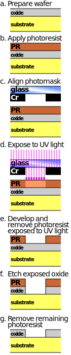 Simplified illustration of dry etching using positive photoresist during a photolithography process in semiconductor microfabrication. Note: Not to scale.
A single iteration of photolithography combines several steps in sequence. Modern cleanrooms use automated, robotic wafer track systems to coordinate the process. The procedure described here omits some advanced treatments, such as thinning agents or edge-bead removal.[1]
Cleaning
If organic or inorganic contaminations are present on the wafer surface, they are usually removed by wet chemical treatment, e.g. the RCA clean procedure based on solutions containing hydrogen peroxide.
Preparation
The wafer is initially heated to a temperature sufficient to drive off any moisture that may be present on the wafer surface. Wafers that have been in storage must be chemically cleaned to remove contamination. A liquid or gaseous "adhesion promoter", such as Bis(trimethylsilyl)amine ("hexamethyldisilazane", HMDS), is applied to promote adhesion of the photoresist to the wafer. The surface layer of silicon dioxide on the wafer reacts with HMDS to form tri-methylated silicon-dioxide, a highly water repellent layer not unlike the layer of wax on a car's paint. This water repellent layer prevents the aqueous developer from penetrating between the photoresist layer and the wafer's surface, thus preventing so-called lifting of small photoresist structures in the (developing) pattern.
Photoresist application
The wafer is covered with photoresist by spin coating. A viscous, liquid solution of photoresist is dispensed onto the wafer, and the wafer is spun rapidly to produce a uniformly thick layer. The spin coating typically runs at 1200 to 4800 rpm for 30 to 60 seconds, and produces a layer between 0.5 and 2.5 micrometres thick. The spin coating process results in a uniform thin layer, usually with uniformity of within 5 to 10 nanometres. This uniformity can be explained by detailed fluid-mechanical modelling, which shows that the resist moves much faster at the top of the layer than at the bottom, where viscous forces bind the resist to the wafer surface. Thus, the top layer of resist is quickly ejected from the wafer's edge while the bottom layer still creeps slowly radially along the wafer. In this way, any 'bump' or 'ridge' of resist is removed, leaving a very flat layer. Final thickness is also determined by the evaporation of liquid solvents from the resist. For very small, dense features (<125 or so nm), thinner resist thicknesses (<0.5 micrometres) are needed to overcome collapse effects at high aspect ratios; typical aspect ratios are <4:1.
The photo resist-coated wafer is then prebaked to drive off excess photoresist solvent, typically at 90 to 100 °C for 30 to 60 seconds on a hotplate.
Exposure and developing
After prebaking, the photoresist is exposed to a pattern of intense light. Optical lithography typically uses ultraviolet light (see below). Positive photoresist, the most common type, becomes soluble in the basic developer when exposed; exposed negative photoresist becomes insoluble in the (organic) developer. This chemical change allows some of the photoresist to be removed by a special solution, called "developer" by analogy with photographic developer. To learn more about the process of exposure and development of positive resist, see, for example: Ralph Dammel, "Diazonaphtoquinone-based resists", SPIE Optical Engineering Press, Vol TT11 (1993).
A PEB (post-exposure bake) is performed before developing, typically to help reduce standing wave phenomena caused by the destructive and constructive interference patterns of the incident light. In DUV (deep ultraviolet, or shorter than 300 nm exposure wavelength) lithography, CAR (chemically amplified resist) chemistry is used. This process is much more sensitive to PEB time, temperature, and delay, as most of the "exposure" reaction (creating acid, making the polymer soluble in the basic developer) actually occurs in the PEB.[2]
The develop chemistry is delivered on a spinner, much like photoresist. Developers originally often contained sodium hydroxide (NaOH). However, sodium is considered an extremely undesirable contaminant in MOSFET fabrication because it degrades the insulating properties of gate oxides (specifically, sodium ions can migrate in and out of the gate, changing the threshold voltage of the transistor and making it harder or easier to turn the transistor on over time). Metal-ion-free developers such as tetramethylammonium hydroxide (TMAH) are now used.
The resulting wafer is then "hard-baked" if a non-chemically amplified resist was used, typically at 120 to 180 °C[citation needed] for 20 to 30 minutes. The hard bake solidifies the remaining photoresist, to make a more durable protecting layer in future ion implantation, wet chemical etching, or plasma etching.
Etching
-
Main article: Etching (microfabrication)
In etching, a liquid ("wet") or plasma ("dry") chemical agent removes the uppermost layer of the substrate in the areas that are not protected by photoresist. In semiconductor fabrication, dry etching techniques are generally used, as they can be made anisotropic, in order to avoid significant undercutting of the photoresist pattern. This is essential when the width of the features to be defined is similar to or less than the thickness of the material being etched (i.e. when the aspect ratio approaches unity). Wet etch processes are generally isotropic in nature, which is often indispensable for microelectromechanical systems, where suspended structures must be "released" from the underlying layer.
The development of low-defectivity anisotropic dry-etch process has enabled the ever-smaller features defined photolithographically in the resist to be transferred to the substrate material.
Photoresist removal
After a photoresist is no longer needed, it must be removed from the substrate. This usually requires a liquid "resist stripper", which chemically alters the resist so that it no longer adheres to the substrate. Alternatively, photoresist may be removed by a plasma containing oxygen, which oxidizes it. This process is called ashing, and resembles dry etching.
Exposure ("printing") systems
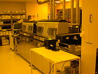 The wafer track portion of an aligner that uses 365 nm ultraviolet light
Exposure systems typically produce an image on the wafer using a photomask. The light shines through the photomask, which blocks it in some areas and lets it pass in others. (Maskless lithography projects a precise beam directly onto the wafer without using a mask, but it is not widely used in commercial processes.) Exposure systems may be classified by the optics that transfer the image from the mask to the wafer.
Contact and proximity
Main article: Contact lithographyA contact printer, the simplest exposure system, puts a photomask in direct contact with the wafer and exposes it to a uniform light. A proximity printer puts a small gap between the photomask and wafer. In both cases, the mask covers the entire wafer, and simultaneously patterns every die.
Contact printing is liable to damage both the mask and the wafer, and this was the primary reason it was abandoned for high volume production. Both contact and proximity lithography require the light intensity to be uniform across an entire wafer, and the mask to align precisely to features already on the wafer. As modern processes use increasingly large wafers, these conditions become increasingly difficult.
Research and prototyping processes often use contact or proximity lithography, because it uses inexpensive hardware and can achieve high optical resolution. The resolution in proximity lithography is approximately the square root of the product of the wavelength and the gap distance. Hence, except for projection lithography (see below), contact printing offers the best resolution, because its gap distance is approximately zero (neglecting the thickness of the photoresist itself). In addition, nanoimprint lithography may revive interest in this familiar technique, especially since the cost of ownership is expected to be low; however, the shortcomings of contact printing discussed above remain as challenges.
Projection
See also: StepperVery-large-scale integration (VLSI) lithography uses projection systems. Unlike contact or proximity masks, which cover an entire wafer, projection masks (known as "reticles") show only one die or an array of die (known as a "field"). Projection exposure systems (steppers or scanners) project the mask onto the wafer many times to create the complete pattern.
Photomasks
-
Main article: Photomask
The image for the mask originates from a computerized data file. This data file is converted to a series of polygons and written onto a square fused quartz substrate covered with a layer of chrome using a photolithographic process. A laser beam (laser writer) or a beam of electrons (e-beam writer) is used to expose the pattern defined by the data file and travels over the surface of the substrate in either a vector or raster scan manner. Where the photoresist on the mask is exposed, the chrome can be etched away, leaving a clear path for the illumination light in the stepper/scanner system to travel through.
Resolution in projection systems
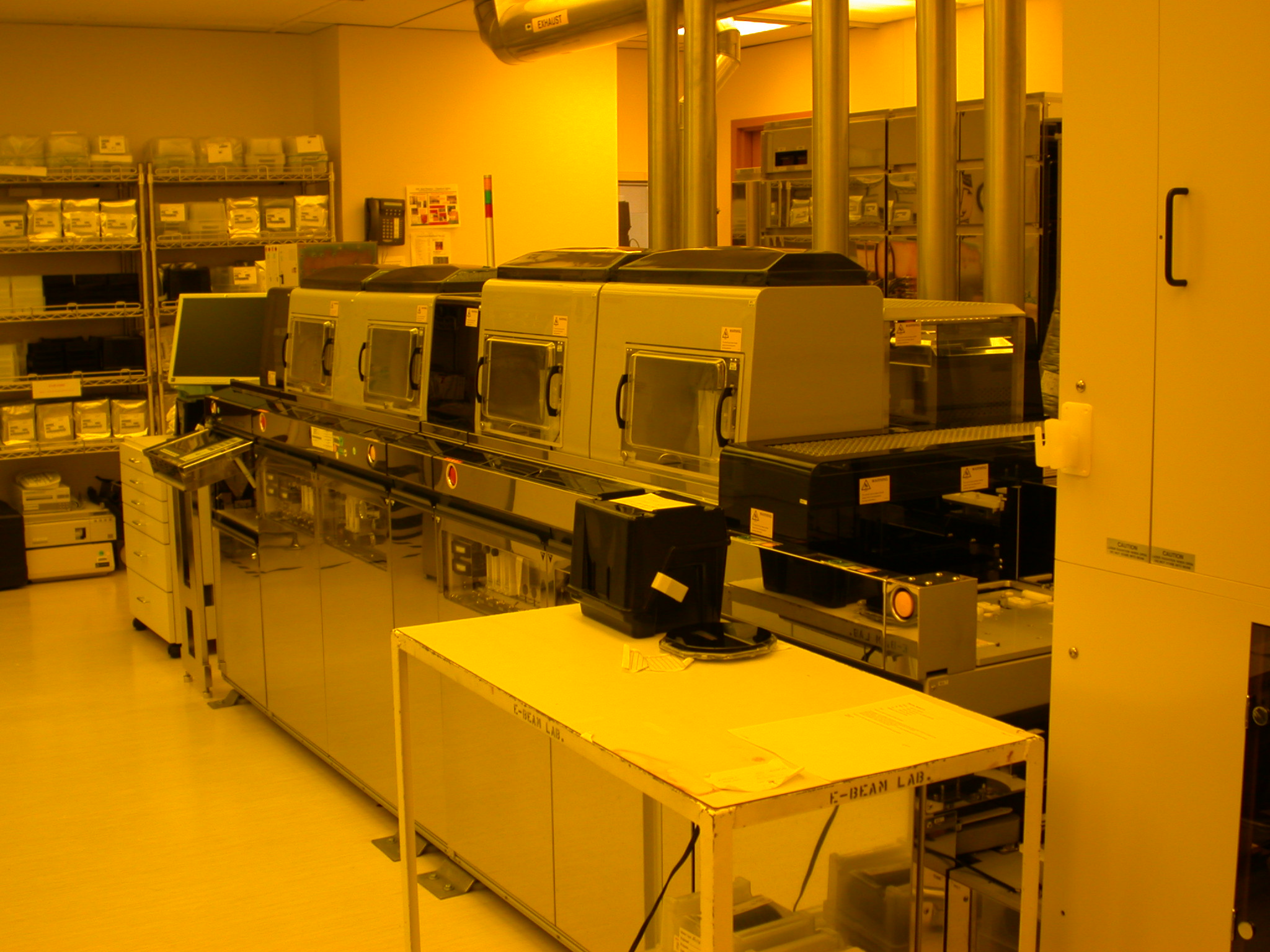
 The filtered fluorescent lighting in photolithography cleanrooms contains no ultraviolet or blue light in order to avoid exposing photoresists. The spectrum of light emitted by such fixtures gives virtually all such spaces a bright yellow color.
The ability to project a clear image of a small feature onto the wafer is limited by the wavelength of the light that is used, and the ability of the reduction lens system to capture enough diffraction orders from the illuminated mask. Current state-of-the-art photolithography tools use deep ultraviolet (DUV) light from excimer lasers with wavelengths of 248 and 193 nm (the dominant lithography technology today is thus also called "excimer laser lithography"), which allow minimum feature sizes down to 50 nm. Excimer laser lithography has thus played a critical role in the continued advance of the so-called Moore’s Law for the last 20 years (see below[3]).
The minimum feature size that a projection system can print is given approximately by:
where
 is the minimum feature size (also called the critical dimension, target design rule). It is also common to write 2 times the half-pitch.
 (commonly called k1 factor) is a coefficient that encapsulates process-related factors, and typically equals 0.4 for production. The minimum feature size can be reduced by decreasing this coefficient through Computational lithography.
 is the wavelength of light used
 is the numerical aperture of the lens as seen from the wafer
According to this equation, minimum feature sizes can be decreased by decreasing the wavelength, and increasing the numerical aperture (to achieve a tighter focused beam and a smaller spot size). However, this design method runs into a competing constraint. In modern systems, the depth of focus is also a concern:
Here,
 is another process-related coefficient. The depth of focus restricts the thickness of the photoresist and the depth of the topography on the wafer. Chemical mechanical polishing is often used to flatten topography before high-resolution lithographic steps.
Light sources
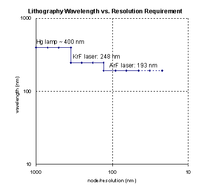
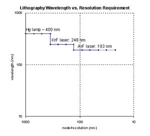 One of the evolutionary paths of lithography has been the use of shorter wavelengths. It is worth noting that the same light source may be used for several technology generations.
Historically, photolithography has used ultraviolet light from gas-discharge lamps using mercury, sometimes in combination with noble gases such as xenon. These lamps produce light across a broad spectrum with several strong peaks in the ultraviolet range. This spectrum is filtered to select a single spectral line. From the early 1960’s through the mid-1980’s, Hg lamps had been used in lithography for their spectral lines at 436 nm ("g-line"), 405 nm ("h-line") and 365 nm ("i-line"). However, with the semiconductor industry’s need for both higher resolution (to produce denser and faster chips) and higher throughput (for lower costs), the lamp-based lithography tools were no longer able to meet the industry’s requirements.
This challenge was overcome when in a pioneering development in 1982, excimer laser lithography was proposed and demonstrated at I.B.M. by K. Jain,[4][5][6][7] and now excimer laser lithography machines (steppers and scanners) are the primary tools used worldwide in microelectronics production. With phenomenal advances made in tool technology in the last two decades, it is the semiconductor industry view[3] that excimer laser lithography has been a crucial factor in the continued advance of Moore’s Law, enabling minimum features sizes in chip manufacturing to shrink from 0.5 micrometer in 1990 to 45 nanometers and below in 2010. This trend is expected to continue into this decade for even denser chips, with minimum features approaching 10 nanometers. From an even broader scientific and technological perspective, in the 50-year history of the laser since its first demonstration in 1960, the invention and development of excimer laser lithography has been highlighted as one of the major milestones.[8][9][10]
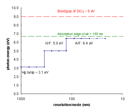
The commonly used deep ultraviolet excimer lasers in lithography systems are the Krypton fluoride laser at 248-nm wavelength and the argon fluoride laser at 193-nm wavelength. The primary manufacturers of excimer laser light sources in the 1980’s were Lambda Physik (now part of Coherent, Inc.) and Lumonics, but since the mid-1990’s Cymer Inc. has become the dominant supplier of excimer laser sources to the lithography equipment manufacturers. Generally, an excimer laser is designed to operate with a specific gas mixture; therefore, changing wavelength is not a trivial matter, as the method of generating the new wavelength is completely different, and the absorption characteristics of materials change. For example, air begins to absorb significantly around the 193 nm wavelength; moving to sub-193 nm wavelengths would require installing vacuum pump and purge equipment on the lithography tools (a significant challenge). Furthermore, insulating materials such as silicon dioxide (SiO2), when exposed to photons with energy greater than the band gap, release free electrons and holes which subsequently cause adverse charging.
Optical lithography has been extended to feature sizes below 50 nm using the 193 nm ArF excimer laser and liquid immersion techniques. Also termed immersion lithography, this enables the use of optics with numerical apertures exceeding 1.0. The liquid used is typically ultra-pure, deionised water, which provides for a refractive index above that of the usual air gap between the lens and the wafer surface. The water is continually circulated to eliminate thermally-induced distortions. Water will only allow NA's of up to ~1.4, but materials with higher refractive indices will allow the effective NA to be increased further.
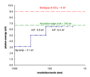 Changing the lithography wavelength is significantly limited by absorption. Air absorbs below ~ 185 nm.
Experimental tools using the 157 nm wavelength from the F2 excimer laser in a manner similar to current exposure systems have been built. These were once targeted to succeed 193 nm lithography at the 65 nm feature size node but have now all but been eliminated by the introduction of immersion lithography. This was due to persistent technical problems with the 157 nm technology and economic considerations that provided strong incentives for the continued use of 193 nm excimer laser lithography technology. High-index immersion lithography is the newest extension of 193 nm lithography to be considered. In 2006, features less than 30 nm were demonstrated by IBM using this technique.[11]
Experimental methods
See also: NanolithographyPhotolithography has been defeating predictions of its demise for many years. For instance, by the early 1980's, many in the semiconductor industry had come to believe that features smaller than 1 micrometer could not be printed optically. Modern techniques using excimer laser lithography already print features with dimensions a fraction of the wavelength of light used - an amazing optical feat. New tricks such as immersion lithography, dual-tone resist and multiple patterning continue to improve the resolution of 193nm lithography. Meanwhile, current research is exploring alternatives to conventional UV, such as electron beam lithography, X-ray lithography, extreme ultraviolet lithography and ion projection lithography.
See also
- Alternative types of lithography
- Excimer lasers
- Moore's law
- Computational lithography
- Stereolithography, a macroscale process used to produce three-dimensional shapes
- Wafer foundry
References
- ^ Jaeger, Richard C. (2002). "Lithography". Introduction to Microelectronic Fabrication. Upper Saddle River: Prentice Hall. ISBN 0-201-44494-7.
- ^ Nalamasu, Omkaram, et al.. "An Overview of Resist Processing for DUV Photolithography". http://www.journalarchive.jst.go.jp/jnlpdf.php?cdjournal=photopolymer1988&cdvol=4&noissue=3&startpage=299&lang=en&from=jnlabstract.
- ^ a b La Fontaine, B., “Lasers and Moore’s Law”, SPIE Professional, Oct. 2010, p. 20; http://spie.org/x42152.xml
- ^ Jain, K. “Excimer Laser Lithography”, SPIE Press, Bellingham, WA, 1990.
- ^ Jain, K. et al., “Ultrafast deep-UV lithography with excimer lasers”, IEEE Electron Device Lett., Vol. EDL-3, 53 (1982): http://ieeexplore.ieee.org/xpl/freeabs_all.jsp?arnumber=1482581
- ^ Lin, B. J., "Optical Lithography", SPIE Press, Bellingham, WA, 2009, p. 136.
- ^ Basting, D., et al., “Historical Review of Excimer Laser Development,” in "Excimer Laser Technology", D. Basting and G. Marowsky, Eds., Springer, 2005.
- ^ American Physical Society / Lasers / History / Timeline; http://www.laserfest.org/lasers/history/timeline.cfm
- ^ SPIE / Advancing the Laser / 50 Years and into the Future; http://spie.org/Documents/AboutSPIE/SPIE%20Laser%20Luminaries.pdf
- ^ U.K. Engineering & Physical Sciences Research Council / Lasers in Our Lives / 50 Years of Impact; http://www.stfc.ac.uk/Resources/PDF/Lasers50_final1.pdf
- ^ Hand, Aaron. "High-Index Lenses Push Immersion Beyond 32 nm". http://www.reed-electronics.com/semiconductor/article/CA6319061.
External links
- BYU Photolithography Resources
- Semiconductor Lithography — Overview of lithography
- Optical Lithography Introduction — IBM site with lithography-related articles
- Immersion Lithography Article — Shows how depth-of-focus is increased with immersion lithography
- Photolithography Equipment- UV Light Shields & Information
- Photo Etching Experts
Categories:- Lithography (microfabrication)
- Microtechnology
-


Wikimedia Foundation. 2010.