- PDP-8
-
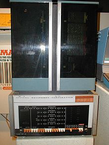 A PDP-8 on display at the Smithsonian's National Museum of American History in Washington, D.C.. This example is from the first generation of PDP-8s, built with discrete transistors and later known as the Straight 8.
The 12-bit PDP-8 was the first successful commercial minicomputer, produced by Digital Equipment Corporation (DEC) in the 1960s. DEC introduced it on 22 March 1965, and sold more than 50,000 systems, the most of any computer up to that date.[1] It was the first widely sold computer in the DEC PDP series of computers (the PDP-5 was not originally intended to be a general-purpose computer). The chief engineer who designed the initial version of the PDP-8 was Edson de Castro, who later founded Data General.[2]
The earliest PDP-8 model (informally known as a "Straight-8") used diode-transistor logic, packaged on flip chip cards, and was about the size of a minibar-fridge.
This was followed by the PDP-8/S, available in desktop and rack-mount models. By using a one-bit serial ALU implementation, the PDP-8/S was smaller, less expensive, but vastly slower than the original PDP-8. The only mass storage peripheral available for the PDP-8/S was the DF32 disk.
Later systems (the PDP-8/I and /L, the PDP-8/E, /F, and /M, and the PDP-8/A) returned to a faster, fully parallel implementation but used much less-expensive TTL MSI logic. Most surviving PDP-8s are from this era. The PDP-8/E is common, and well-regarded because so many types of I/O devices were available for it. It was often configured as a general-purpose computer.
In 1975, early personal computers based on inexpensive microprocessors, such as the MITS Altair and later TRS-80, Apple II and others began to dominate the market for small general purpose computers.
The last commercial PDP-8 models in 1979 were called "CMOS-8s" and used custom CMOS microprocessors. They were not priced competitively, and the offering failed. The IBM PC in 1981 cemented the doom of the CMOS-8s by making a legitimate, well-supported small microprocessor computer.
Intersil sold the integrated circuits commercially through to 1982 as the Intersil 6100 family. By virtue of their CMOS technology they had low power requirements and were used in some embedded military systems.
Contents
Architectural significance
The PDP-8 combined low cost, simplicity, expandability and careful engineering for value. The greatest historical significance was that the PDP-8's low cost and high volume made a computer available to many new uses and people. Its continuing significance is as a historical example of value-engineered computer design.
The low complexity brought other costs. It made programming cumbersome, as is seen in the examples in this article and from the discussion of "pages" and "fields." Some ambitious programming projects failed to fit in memory or developed design defects that could not be solved.
As design advances reduced the costs of logic and memory, the programmer's time became more important. Subsequent computer designs emphasized ease of programming, typically using a larger and more intuitive instruction set.
Eventually, most machine-language programming came to be generated by compilers and report generators. The reduced instruction set computer returned full-circle to the PDP-8's emphasis on a simple instruction set and achieving multiple actions in a single instruction cycle, in order to maximize execution speed, though the newer computers had much longer instruction words.
Description
The PDP-8 used ideas from several 12-bit predecessors, most notably the LINC designed by W.A. Clark and C.E. Molnar who were inspired by Seymour Cray's CDC 160 minicomputer.[3]
The architecture had a simple programmed I/O bus, plus a DMA channel. The programmed I/O bus would typically run low to medium-speed peripherals, such as printers, teletypes, paper tape punches and readers, while DMA was used for cathode ray tube screens with a light pen, analog-to-digital converters, digital-to-analog converters, tape drives, disk drives.
The word size, 12 bits, is large enough to handle unsigned integers from 0 to 4095 – wide enough for controlling simple machinery. This is also enough to handle signed numbers from -2048 to +2047. This is higher precision than a slide rule or most analog computers. Twelve bits could also store two six-bit ASCII subset characters.
To save money, the design uses inexpensive main memory for many purposes that are served by more expensive flip-flop registers in other computers.[4]
The PDP-8's basic configuration had a main memory of 4,096 twelve-bit words. An optional memory-expansion unit could switch banks of such memories using the IOT instruction.
At its inception, the programmer's view of the PDP-8 had only eight instructions and two registers (a 12-bit accumulator, AC, and a carry bit called the "link register", L). The machine used magnetic core memory with a cycle time of 1.5 microseconds, so that a typical two-cycle (Fetch, Execute) memory-reference instruction ran at a speed of 0.333 MIPS. The 1974 Pocket Reference Card gave a basic instruction time of 1.2 microseconds, or 2.6 microseconds for instructions that referenced memory. Later machines added a second register (the Multiplier/Quotient Register, MQ). An extended arithmetic element option added actual multiply and divide instructions.
The PDP-8 was optimized for simplicity of design. The CPU of the serial model, the PDP-8/S, had only about 519 logic gates, while small microcontrollers (as of 2008) usually have 15,000 or more. Compared to more complex machines, unnecessary features were removed, and logic was shared when possible. Instructions used autoincrement, autoclear and indirect access to increase the software's speed, reduce memory use and substitute inexpensive memory for expensive registers. A basic PDP-8 CPU has only four 12-bit registers, the accumulator, program counter, memory-buffer register and memory-address register. To save money, these were all used for multiple purposes at different points in the operating cycle. For example, the memory buffer register provided arithmetic operands, was part of the instruction register, and stored data to rewrite the core memory. (This restores the core data destroyed by the read.) In spite of its basic simplicity, the use of very small modules made it an expensive machine, with a large part of the cost sunk into the small modules, the thousands of gold-plated connectors, and the complex wire-wrapped backplane. In the 8/S two different logic voltages were used, an inexpensive way to increase the fan-out of the inexpensive diode-transistor logic.[5]
Versions of the PDP-8
 PDP-8/E front panel
The total sales figure for the PDP-8 family has been estimated at over 300,000 machines. The following models were manufactured:
- PDP-8
- LINC-8
- PDP-8/S
- PDP-8/I
- PDP-8/L
- PDP-12
- PDP-8/E
- PDP-8/F
- PDP-8/M
- PDP-8/A
- Intersil 6100 single-chip PDP-8-compatible microprocessor (used in the VT78)
- Harris 6120 CMOS single-chip PDP-8-compatible microprocessor (used in the DECmate word processors)
Latter-day implementations
Enthusiasts have created entire PDP-8 systems using single FPGA devices. (This is possible because an entire PDP-8, its main memory system, and its I/O equipment is collectively much less complex than even the cache memories used in most modern microprocessors.)
Several software simulations of a PDP-8 are available on the Internet. The best of these correctly execute DEC's diagnostic software, and run historic operating systems and software. The software simulations often simulate late "large" PDP-8 systems with all possible peripherals. Even these use only a tiny fraction of the capacity of a modern personal computer.
Input/Output
The I/O systems underwent huge changes during the PDP-8 era. Early PDP-8 models used a front panel interface, a paper-tape reader and a teletype printer with an optional paper-tape punch. Over time I/O systems such as magnetic tape, RS-232 and current loop dumb terminals, punched card readers, and fixed-head disks were added. Toward the end of the PDP-8 era, floppy disks and moving-head cartridge disk drives were popular I/O devices. Modern enthusiasts have created standard PC style IDE hard disk adapters for real and simulated PDP-8 computers.
I/O was supported through several different methods:
- In-backplane dedicated slots for I/O controllers
- A "Negative" I/O bus (using negative voltage signalling)
- A "Positive" I/O bus (the same architecture using TTL signalling)
- The Omnibus (a backplane of undedicated system bus slots) introduced in the PDP-8/E
A simplified, inexpensive form of DMA called "three-cycle data break" was supported; this required the assistance of the processor. The "data break" method moved some of common logic needed to implement DMA I/O from each I/O device into one common copy of the logic within the processor. "Data break" placed the processor in charge of maintaining the DMA address and word count registers. In three successive memory cycles, the processor would update the word count, update the transfer address, and store or retrieve the actual I/O data word.
One cycle data break effectively tripled the DMA transfer rate because only the target data needed to be transferred to and from the core memory. However, the I/O devices needed more electronic logic to manage their own word count and transfer address registers. By the time the PDP-8/E was introduced, electronic logic had become less expensive and "one-cycle data break" became more popular.
Programming facilities
Early PDP-8 systems did not have an operating system, just a front panel and run and halt switches. Software development systems for the PDP-8 series began with the most basic front panel entry of raw binary machine code (booting entry).
In the middle era, various paper tape "operating systems" were developed. Many utility programs became available on paper tape. PAL-8 assembly language source code was often stored on paper tape, read into memory, and saved to paper tape. PAL assembled from paper tape into memory. Paper tape versions of a number of programming languages were available, including DEC's FOCAL interpreter and a 4K FORTRAN compiler and runtime.
Toward the end of the PDP-8 era, operating systems such as OS/8 and COS-310 allowed a traditional line mode editor and command-line compiler development system using languages such as PAL-III assembly language, FORTRAN, BASIC, and DIBOL.
Fairly modern and advanced RTOS and preemptive multitasking multi-user systems were available: a real-time system (RTS-8) was available as were multiuser commercial systems (COS-300 and COS-310) and a dedicated single-user word-processing system (WPS-8).
A time-sharing system, TSS-8, was also available. TSS-8 allowed multiple users to log into the system via 110-baud terminals, and edit, compile and debug programs. Languages included a special version of BASIC, a FORTRAN subset similar to FORTRAN-1 (no user-written subroutines or functions), an ALGOL subset, FOCAL, and an assembler called PAL-D.
A fair amount of user-donated software for the PDP-8 was available from DECUS, the Digital Equipment Corporation User Society, and often came with full source listings and documentation.
Instruction set
The three high-order bits of the 12-bit instruction word (labelled bits 0 through 2) are the operation code. For the six operations that refer to memory, bits 5 through 11 provide a 7-bit address. Bit 4, if set, says to complete the address using the 5 high-order bits of the PC; if clear, zeroes are used. Bit 3 specifies indirection; if set, the address obtained as described so far points to a 12-bit value in memory that gives the actual effective address for the instruction. (The JMP instruction does not operate on a memory word, except if indirection is specified, but has the same bit fields.)
0 2 3 4 5 11 Operation I Z Offset - Memory pages
This use of the instruction word divides the 4,096-word memory into 128-word pages; bit 4 of the instruction selects either the current page or page 0 (addresses 0000–0177 in octal). Memory in page 0 is at a premium, since variables placed here can be addressed directly from any page. (Moreover, address 0000 is where any interrupt service routine must start, and addresses 0010–0017 have the special property of auto-incrementing preceding any indirect reference through them.)
The standard assembler places constant values for arithmetic in the current page. Likewise, cross-page jumps and subroutine calls use an indirect address in the current page.
It was important to write routines to fit within 128-word pages, or to arrange routines to minimize page transitions, as references and jumps outside the current page required an extra word. Consequently, much time was spent cleverly conserving one or several words. Programmers deliberately placed code at the end of a page to achieve a free transition to the next page as PC was incremented.
Basic instructions
- 000 – AND – AND the memory operand with AC.
- 001 – TAD – Two's complement ADd the memory operand to <L,AC> (a 13 bit signed value).
- 010 – ISZ – Increment the memory operand and Skip next instruction if result is Zero.
- 011 – DCA – Deposit AC into the memory operand and Clear AC.
- 100 – JMS – JuMp to Subroutine (storing return address in first word of subroutine!).
- 101 – JMP – JuMP.
- 110 – IOT – Input/Output Transfer (see below).
- 111 – OPR – microcoded OPeRations (see below).
IOT (Input-Output Transfer) instructions
The PDP-8 processor defined few of the IOT instructions, but simply provided a framework. Most IOT instructions were defined by the individual I/O devices.
0 2 3 8 9 11 6=IOT Device Function - Device
Bits 3 through 8 of an IOT instruction selected an I/O device. Some of these device addresses were standardized by convention:
- 00 was handled by the processor and not sent to any I/O device (see below)
- 01 was usually the high-speed paper tape reader
- 02 was the high-speed paper tape punch
- 03 was the console keyboard (and any associated low-speed paper tape reader)
- 04 was the console printer (and any associated low-speed paper tape punch)
Instructions for device 0 affected the processor as a whole. For example, ION (6001) enabled interrupt processing, and IOFF (6002) disabled it.
- Function
Bits 9 through 11 of an IOT instruction selected the function(s) the device would perform. Simple devices (such as the paper tape reader and punch and the console keyboard and printer) would use the bits in standard ways:
- Bit 11 caused the processor to skip the next instruction if the I/O device was ready
- Bit 10 cleared AC
- Bit 9 moved a word between AC and the device, initiated another I/O transfer, and cleared the device's "ready" flag
These operations took place in a well-defined order that gave useful results if more than one bit was set.
More complicated devices, such as disk drives, used these 3 bits in device-specific fashions. Typically, a device decoded the 3 bits to give 8 possible function codes.
OPR (OPeRate)
Many operations were achieved using OPR, including most of the conditionals. OPR does not address a memory location; conditional execution is achieved by conditionally skipping one instruction, which was typically a JMP.
The OPR instruction was said to be "microcoded." This did not mean what the word means today (that a lower-level program fetched and interpreted the OPR instruction), but meant that each bit of the instruction word specified a certain action, and the programmer could achieve several actions in a single instruction cycle by setting multiple bits. In use, a programmer would write several instruction mnemonics alongside one another, and the assembler would combine them with OR to devise the actual instruction word. Many I/O devices supported "microcoded" IOT instructions.
Microcoded actions took place in a well-defined sequence designed to maximize the utility of many combinations.
The OPR instructions came in Groups. Bits 3, 8 and 11 identify the Group of an OPR instruction, so it was impossible to combine the microcoded actions from different groups.
Group 1
00 01 02 03 04 05 06 07 08 09 10 11 ___________________________________ | 1| 1| 1| 0| | | | | | | | | |__|__|__|__|__|__|__|__|__|__|__|__| |CLA CMA RAR BSW CLL CML RAL IAC Execution order 1 1 2 2 4 4 4 3- 7200 – CLA – Clear Accumulator
- 7100 – CLL – Clear the L Bit
- 7040 – CMA – Ones Complement Accumulator
- 7020 – CML – Complement L Bit
- 7001 – IAC – Increment <L,AC>
- 7010 – RAR – Rotate <L,AC> Right
- 7004 – RAL – Rotate <L,AC> Left
- 7012 – RTR – Rotate <L,AC> Right Twice
- 7006 – RTL – Rotate <L,AC> Left Twice
- 7002 – BSW – Byte Swap 6-bit "bytes" (PDP 8/e and up)
In most cases, the operations are sequenced so that they can be combined in the most useful ways. For example, combining CLA (CLear Accumulator), CLL (CLear Link), and IAC (Increment ACcumulator) first clears the AC and Link, then increments the accumulator, leaving it set to 1. Adding RAL to the mix (so CLA CLL IAC RAL) causes the accumulator to be cleared, incremented, then rotated left, leaving it set to 2. In this way, small integer constants were placed in the accumulator with a single instruction.
The combination CMA IAC, which the assembler let you abbreviate as CIA, produced the arithmetic inverse of AC: the twos-complement negation. Since there was no subtraction instruction, only the twos-complement add (TAD), computing the difference of two operands required first negating the subtrahend.
A Group 1 OPR instruction that has none of the microprogrammed bits set performs no action. The programmer can write NOP (No Operation) to assemble such an instruction.
Group 2, Or Group
00 01 02 03 04 05 06 07 08 09 10 11 ___________________________________ | 1| 1| 1| 1| | | | | 0| | | 0| |__|__|__|__|__|__|__|__|__|__|__|__| |CLA SZA OSR SMA SNL HLT 2 1 1 1 3 2- 7600 – CLA – Clear AC
- 7500 – SMA – Skip on AC < 0 (or group)
- 7440 – SZA – Skip on AC = 0 (or group)
- 7420 – SNL – Skip on L ≠ 0 (or group)
- 7404 – OSR – logically 'or' front-panel switches with AC
- 7402 – HLT – Halt
When bit 8 is clear, a skip is performed if any of the specified conditions are true. For example "SMA SZA", opcode 7540, skips if AC ≤ 0.
A Group 2 OPR instruction that has none of the microprogrammed bits set is another No-Op instruction.
Group 2, And Group
00 01 02 03 04 05 06 07 08 09 10 11 ___________________________________ | 1| 1| 1| 1| | | | | 1| | | 0| |__|__|__|__|__|__|__|__|__|__|__|__| |CLA SNA OSR SPA SZL HLT 2 1 1 1 3 2- 7410 – SKP – Skip Unconditionally
- 7610 – CLA – Clear AC
- 7510 – SPA – Skip on AC ≥ 0 (and group)
- 7450 – SNA – Skip on AC ≠ 0 (and group)
- 7430 – SZL – Skip on L = 0 (and group)
When bit 8 is set, the Group 1 skip condition is inverted: the skip is not performed if any of the group 1 conditions are true, meaning that all of the specified skip conditions must be true. For example, "SPA SNA", opcode 7550, skips if AC > 0. If none of bits 5–7 are set, then the skip is unconditional.
Group 3
Unused bit combinations of OPR were defined as a third Group of microprogrammed actions mostly affecting the MQ (Multiplier/Quotient) register.
00 01 02 03 04 05 06 07 08 09 10 11 ___________________________________ | 1| 1| 1| 1| | | | | | | | 1| |__|__|__|__|__|__|__|__|__|__|__|__| |CLA SCA \_ _/ | MQA MQL CODE 1* 2 2 2 3- 7601 – CLA – Clear AC
- 7501 – MQA – Multiplier Quotient with AC (logical or MQ into AC)
- 7441 – SCA – Step counter load into AC
- 7421 – MQL – Multiplier Quotient Load (Transfer AC to MQ, clear AC)
- 7621 – CAM – CLA + MQL clears both AC and MQ.
Typically CLA and MQA were combined to transfer MQ into AC. Another useful combination is MQA and MQL, to exchange the two registers.
Three bits specified a multiply/divide instruction to perform:
- 7401 – No operation
- 7403 – SCL – Step Counter Load (immediate word follows, PDP-8/I and up)
- 7405 – MUY – Multiply
- 7407 – DVI – Divide
- 7411 – NMI – Normalize
- 7413 – SHL – Shift left (immediate word follows)
- 7415 – ASR – Arithmetic shift right
- 7417 – LSR – Logical shift right
Memory control
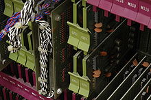 PDP-8/I core stack
A 12-bit word can have 4,096 different values, and this was the maximum number of words the original PDP-8 could address indirectly through a word pointer. As programs became more complex and the price of memory fell, it became desirable to expand this limit. To maintain compatibility with pre-existing programs, the designers chose the approach of using hardware outside the original design to add high-order bits to the effective addresses generated by the program.
Consequently, adding a "Memory Extension Controller" expanded the addressable memory by a factor of 8, to a total of 32,768 words. This expansion was thought sufficient because, with core memory then costing about 50 cents a word, a full 32K of memory would equal the cost of the CPU.
Each 4K of memory was called a "field." The Memory Extension Controller contained two three-bit registers: the DF (Data Field) and the IF (Instruction Field). These registers specified a field for each memory reference of the CPU, allowing a total of 15 bits of address. The IF register specified the field for instruction fetches and direct memory references; the DF register specified the field for indirect data accesses. A program running in one field could reference data in the same field by direct addressing, and reference data in another field by indirect addressing.
A set of IO instructions in the range 6200 through 6277 was handled by the Memory Extension Controller and gave access to the DF and IF registers. The 62X1 instruction (CDF, Change Data Field) set the data field to X. Similarly 62X2 (CIF) set the instruction field, and 62X3 set both. Pre-existing programs would never execute CIF or CDF; the DF and IF registers would both point to the same field, a single field to which these programs were limited.
It was more complicated for multiple-field programs to deal with field boundaries and the DF and IF registers than it would have been if they could simply generate 15-bit addresses, but the design provided backward compatibility and was consistent with the 12-bit architecture used throughout the PDP-8. Compare the later Intel 8086, whose 16-bit memory addresses are expanded to 20 bits by combining them with the contents of a specified or implied "segment" register.
The effect of the CIF instruction was deferred to coincide with the next JMP or JMS instruction, so that executing CIF would not cause a jump. Additional IO instructions to the Memory Extension Controller retrieved the current value of these registers, letting software save and restore the machine state across an interrupt.
The extended memory scheme let existing programs handle increased memory with minimal changes. For example, 4K FOCAL normally had about 3K of code with only 1K left over for user program and data. With a few patches, FOCAL could use a second 4K field for user program and data. Moreover, additional 4K fields could be allocated to separate users, turning 4K FOCAL into a multi-user timesharing system.
- Virtualization
On the PDP-8/E and later models, the Extended Memory Controller was enhanced to enable machine virtualization. A program written to use a PDP-8's entire resources could coexist with other such programs on the same PDP-8 under the control of a virtual machine manager. The manager would order all I/O instructions (including those that operated on the Extended Memory Controller) to cause a trap (an interrupt handled by the manager). In this way, the manager could map memory references, map data or instruction fields, and redirect I/O to different devices. Each original program had complete access to a "virtual machine" provided by the manager.
There was one problem with virtualization: Whether the CPU was in the process of deferring the effect of a CIF instruction (whether it had executed a CIF and not yet executed the matching jump instruction) was something that a program could not sense or modify. So the manager could not completely restore the machine state. The manager had to include a complete PDP-8 emulator (not difficult for an 8-instruction machine). Whenever a CIF instruction trapped to the manager, it had to emulate the instructions up to the next jump. Fortunately, as a jump usually was the next instruction after CIF, this emulation did not slow programs down much, but it is a large workaround to a seemingly small design deficiency.
By the time of the PDP-8/A, memory prices had fallen enough that 32K was not a huge budgetary item and more memory was desirable. The 8/A added a new set of instructions for handling more than eight fields of memory. The field number could now be placed in the AC, rather than having to be hard-coded into the instruction. However, by this time, the PDP-8 was in decline, so very little standard software was modified to use these new features.
Examples
The following examples show code in PDP-8 assembly language as one might write for the PAL-III assembler.
Comparing two numbers
The following piece of code shows what is needed just to compare two numbers:
    /Compare numbers in memory at OPD1 and OPD2
            CLA CLL     /Must start with 0 in AC and link
            TAD OPD1    /Load first operand into AC (by adding it to 0); link is still clear
            CIA         /Complement, then increment AC, negating it
            TAD OPD2    /AC now has OPD2-OPD1; if OPD2≥OPD1, sum overflows and link is set
            SZL         /Skip if link is clear
            JMP OP2GT   /Jump somewhere in the case that OPD2≥OPD1;
                        /Otherwise, fall through to code below.
As shown, much of the text of a typical PDP-8 program focuses not on the author's intended algorithm but on low-level mechanics. An additional readability problem is that in conditional jumps such as the one shown above, the conditional instruction (which skips around the JMP) highlights the opposite of the condition of interest.
String output
This complete PDP-8 assembly language program outputs "Hello, world!" to the teleprinter.
    *10                   / Set current assembly origin to address 10,
    STPTR,    STRNG-1     / An auto-increment register (one of eight at 10-17)

    *200                  / Set current assembly origin to program text area
    HELLO,  CLA CLL       / Clear AC and Link again (needed when we loop back from tls)
            TAD I Z STPTR / Get next character, indirect via PRE-auto-increment address from the zero page
            SNA           / Skip if non-zero (not end of string)
            HLT           / Else halt on zero (end of string)
            TLS           / Output the character in the AC to the teleprinter
            TSF           / Skip if teleprinter ready for character
            JMP .-1       / Else jump back and try again
            JMP HELLO     / Jump back for the next character

    STRNG,  310           / H
            345           / e
            354           / l
            354           / l
            357           / o
            254           /,
            240           / (space)
            367           / w
            357           / o
            362           / r
            354           / l
            344           / d
            241           / !
            0             / End of string
    $HELLO                /DEFAULT TERMINATOR
Subroutines
The PDP-8 processor did not implement a stack upon which to store registers or other context when a subroutine was called or an interrupt occurred. (A stack could be implemented in software, as demonstrated in the next section.) Instead, the JMS instruction simply stored the updated PC (pointing past JMS, to the return address) at the effective address and jumped to the effective address plus one. The subroutine returned to its caller using an indirect JMP instruction that addressed the subroutine's first word.
For example, here is "Hello, World!" re-written to use a subroutine. When the JMS instruction jumps to the subroutine, it modifies the 0 coded at location OUT1:
    *10                     / Set current assembly origin to address 10,
    STPTR,  STRNG-1         / An auto-increment register (one of eight at 10-17)

    *200                    / Set assembly origin (load address)
    LOOP,   TAD I STPTR     / Pre-increment mem location 10, fetch indirect to get the next character of our message
            SNA             / Skip on non-zero AC
            HLT             / Else halt at end of message
            JMS OUT1        / Write out one character
            JMP LOOP        / And loop back for more
    OUT1,   0               / Will be replaced by caller's updated PC
            TSF             / Skip if printer ready
            JMP .-1         / Wait for flag
            TLS             / Send the character in the AC
            CLA CLL         / Clear AC and Link for next pass
            JMP I OUT1      / Return to caller
    STRNG, "H               / A well-known message
           "e               /
           "l               / NOTE:
           "l               /
           "o               /   Strings in PAL-8 and PAL-III were "sixbit"
           ",               /   To use ASCII, we'll have to spell that out, character by character
           "                /
           "w               /
           "o               /
           "r               /
           "l               /
           "d               /
           "!               /
           015              /
           012              /
           0                / Mark the end of our .ASCIZ string ('cause .ASCII hadn't been invented yet!)
The fact that the JMS instruction used the word just before the code of the subroutine to deposit the return address prevented reentrancy and recursion without additional work by the programmer. It also made it difficult to use ROM with the PDP-8 because read-write return-address storage was commingled with read-only code storage in the address space. Programs intended to be placed into ROMs approached this problem in several ways:
- They copied themselves to read-write memory before execution, or
- They were placed into special ROM cards that provided a few words of read/write memory, accessed indirectly through the use of a thirteenth flag bit in each ROM word.
- They avoided the use of subroutines; or used code such as the following, instead of the JMS instruction, to put the return address in read-write memory:
    JUMPL, DCA TEMP         / Deposit the accumulator in some temporary location
           TAD JUMPL+3      / Load the return address into the accumulator: hard coded
           JMP SUBRO        / Go to the subroutine, and have it handle jumping back
           JUMPL+4          / Return address
The use of the JMS instruction made debugging difficult. If a programmer made the mistake of having a subroutine call itself, directly or by an intermediate subroutine, then the return address for the outer call would be destroyed by the return address of the subsequent call, leading to an infinite loop. If one module was coded with an incorrect or obsolete address for a subroutine, it would not just fail to execute the entire code sequence of the subroutine, it might modify a word of the subroutine's code, depositing a return address that the processor might interpret as an instruction during a subsequent correct call to the subroutine. Both types of error might become evident during the execution of code that was written correctly.
Software stack
Though the PDP-8 did not have a hardware stack, it could be implemented in software. Here are example PUSH and POP subroutines, simplified to omit issues such as testing for stack overflow and underflow:
    PUSH, 0
          DCA DATA
          CLA CMA     / -1
          TAD SP
          DCA SP
          TAD DATA
          DCA I SP
          JMP I PUSH     /Return

    POP,  0
          CLA CLL
          TAD I SP
          ISZ SP
          JMP I POP

    DATA, 0
    SP, 0
And here is "Hello World" with this "stack" implemented, and "OUT" subroutine:
    *200
    MAIN,  CLA CLL         /Set the message pointer
           TAD (MESSG      /To the beginning of the message (literal)
           DCA SP

    LOOP,  JMS POP
           SNA             /Stop execution if zero
           HLT
           JMS OUT         /Otherwise, output a character
           JMP LOOP

    MESSG, "H
           "e
           "l
           "l
           "o
           ",
           "
           "w
           "o
           "r
           "l
           "d
           "!
           015
           012
           0

    OUT,    0               / Will be replaced by caller's updated PC
            TSF             / Skip if printer ready
            JMP .-1         / Wait for flag
            TLS             / Send the character in the AC
            CLA CLL         / Clear AC and Link for next pass
            JMP I OUT      / Return to caller
Linked list
Another possible subroutine for the PDP-8 was a linked list.
     GETN, 0     /Gets the number pointed to and moves the pointer
     CLA CLL     /Clear accumulator
     TAD I PTR   /Gets the number pointed to
     DCA TEMP    /Save current value
     ISZ    PTR     /Increment pointer
     TAD I PTR   /Get next address
     DCA PTR     /Put in pointer
     JMP I GETN  /return
     PTR,  0
     TEMP, 0
Interrupts
There was a single interrupt line on the PDP-8 I/O bus and interrupts were processed identically to having called a subroutine at location 0000 except that the interrupt system was also automatically disabled. Just as it was difficult to reentrantly call subroutines, it was difficult to nest interrupts and this was usually not done; each interrupt ran to completion and re-enabled the interrupt system just before executing the JMP I 0 instruction which acted as the exit from the interrupt.
Because there was only a single interrupt line on the I/O bus, the occurrence of an interrupt conveyed no information to the processor about the source of the interrupt. Instead, the interrupt service routine had to serially poll each active I/O device to see if it was the source of the interrupt; the code that did this was usually referred to as a skip chain because it consisted of a lot of PDP-8 "test and skip if flag set" I/O instructions. (It was also not unheard-of for a skip chain to reach its end and not have found any device in need of service.) The relative interrupt priority of the I/O devices was determined by their position in the skip chain with devices nearer the front of the skip chain having higher priority for service.
Books
An engineering textbook popular in the 1980s, The Art of Digital Design by David Winkel and Franklin Prosser, describes the process of designing a computer that is compatible with the PDP-8/I as an exercise. The function of every component is explained. Although it is not a production design, the exercise provides a detailed description of the computer's operation.
Notes
- ^ The Digital Equipment Corporation PDP-8 by Douglas W. Jones
- ^ The ultimate entrepreneur: the story of Ken Olsen and Digital Equipment Corporation entry in Google Books, by Glenn Rifkin, George Harrar, 1988, ISBN 978-1559580229
- ^ Bell, Gordon; C. Mudge, J. McNamara (1978). Computer Engineering: A DEC View of Hardware Systems Design. Digital Press. ISBN 0932376002. http://books.google.com/books?id=rN0iAAAAMAAJ&dq=Computer+Engineering:+A+DEC+View+of+Hardware+Systems+Design&q=Computer+Engineering:+A+DEC+View+of+Hardware+Systems+Design&pgis=1.
- ^ C. Gordon Bell, et al.; Computer Structures, Principles and Organization, 1982, PDP-8 chapter
- ^ PDP-8/S Maintenance Manual, DEC, 1971
References
- C. Gordon Bell and Allen Newell, 1971, Computer Structures: Readings and Examples, McGraw-Hill Book Company, New York. Chapter 5 The DEC PDP-8, pages 120-136. With enough detail that an electrical engineer could build one (if able to find the parts).
External links
- What is a PDP-8?, FAQS.ORG
- pdp-8 Documentation: The Small Computer Handbook (1966 Edition), Sections 1 and 2 and others are available from Simon Fraser University
- PDP-8 Frequently Asked Questions, FAQS.ORG
- http://www.cs.uiowa.edu/~jones/pdp8/
- http://www.faqs.org/faqs/dec-faq/pdp8-models/preamble.html
- pdp8online.com has a running PDP8 that anyone can control through a Java applet, plus a webcam to show the results
- dpa, a portable PDP-8 cross-assembler
- Spare Time Gizmos' SBC6120 PDP-8 compatible computer with optional front panel
- Still working Classic 8, PDP 8e and 8i in a German computer museum
- pdp12.lofty.com contains information on restoring PDP-8s and paper tape resources
- Bernhard Baehr's slick PDP-8/E Simulator for Macintosh
- Willem van der Mark's PDP-8/E Simulator in Java
- http://simh.trailing-edge.com a very portable simulator for PDP-8, works on virtually any modern OS
- The Digital Equipment Corporation PDP-8, 1965 - Computer History Collection from the Smithsonian
- Historic application of PDP8 in Germany for all Deutsche Bank centers and other financial institutes: Olympia Multiplex 80 (Olympia Business Systems)
- http://www.pdp8.co.uk/ Blogs the restoration of PDP-8 computers
- http://www.grc.com/pdp-8/pdp-8.htm Steve Gibson's explanation on how the PDP-8 works and how to program it.
- YouTube has a video series showing the PDP-8
- "Index of PDP-8 documents". BitSavers.Org web site. http://www.bitsavers.org/pdf/dec/pdp8/. Retrieved May 29, 2011.
Digital Equipment Corporation computers PDP VAX x86 MIPS Alpha Categories:- DEC hardware
- Minicomputers
- 1965 introductions
- Transistorized computers
- Instruction set architectures


Wikimedia Foundation. 2010.