- Common base
-
 Figure 1: Basic NPN common-base circuit (neglecting biasing details).
In electronics, a common-base (also known as grounded-base) amplifier is one of three basic single-stage bipolar junction transistor (BJT) amplifier topologies, typically used as a current buffer or voltage amplifier. In this circuit the emitter terminal of the transistor serves as the input, the collector the output, and the base is common to both (for example, it may be tied to ground reference or a power supply rail), hence its name. The analogous field-effect transistor circuit is the common-gate amplifier.
Contents
Applications
This arrangement is not very common in low-frequency circuits, where it is usually employed for amplifiers that require an unusually low input impedance, for example to act as a preamplifier for moving-coil microphones. However, it is popular in high-frequency amplifiers, for example for VHF and UHF, because its input capacitance does not suffer from the Miller effect, which degrades the bandwidth of the common-emitter configuration, and because of the relatively high isolation between the input and output. This high isolation means that there is little feedback from the output back to the input, leading to high stability.
This configuration is also useful as a current buffer since it has a current gain of approximately unity (see formulas below). Often a common base is used in this manner, preceded by a common-emitter stage. The combination of these two form the cascode configuration, which possesses several of the benefits of each configuration, such as high input impedance and isolation.
Low-frequency characteristics
At low frequencies and under small-signal conditions, the circuit in Figure 1 can be represented by that in Figure 2, where the hybrid-pi model for the BJT has been employed. The input signal is represented by a Thévenin voltage source, vs, with a series resistance Rs and the load is a resistor RL. This circuit can be used to derive the following characteristics of the common-base amplifier.
Definition Expression Approximate expression Conditions Open-circuit voltage gain 


Short-circuit current gain 

1 
Input resistance 


Output resistance 
![R_C \| \{[1+g_m (r_{\pi}\|R_S) ]r_O +(r_{\pi}\|R_S)\}](7/fe7d78660d054ff51c0a28f37966a374.png)
RC | | rO 
- Note: Parallel lines (||) indicate components in parallel.
In general the overall voltage/current gain may be substantially less than the open/short circuit gains listed above (depending on the source and load resistances) due to the loading effect.
Active loads
For voltage amplification, the range of allowed output voltage swing in this amplifier is tied to its voltage gain when a resistor load RC is employed, as in Figure 1. That is, large voltage gain requires large RC, and that in turn implies a large DC voltage drop across RC. For a given supply voltage, the larger this drop, the smaller the transistor VCB and the less output swing is allowed before saturation of the transistor occurs, with resultant distortion of the output signal. To avoid this situation, an active load can be used, for example, a current mirror. If this choice is made, the value of RC in the table above is replaced by the small-signal output resistance of the active load, which is generally at least as large as the rO of the active transistor in Figure 1. On the other hand, the DC voltage drop across the active load is a fixed low value (the compliance voltage of the active load), much less than the DC voltage drop incurred for comparable gain using a resistor RC. That is, an active load imposes less restriction on the output voltage swing. Notice that active load or not, large AC gain still is coupled to large AC output resistance, which leads to poor voltage division at the output except for large loads RL >> Rout.
For use as a current buffer, gain is not affected by RC, but output resistance is. Because of the current division at the output, it is desirable to have an output resistance for the buffer much larger than the load RL being driven so large signal currents can be delivered to a load. If a resistor RC is used, as in Figure 1, a large output resistance is coupled to a large RC, again limiting the signal swing at the output. (Even though current is delivered to the load, usually a large current signal into the load implies a large voltage swing across the load as well.) An active load provides high AC output resistance with much less serious impact upon the amplitude of output signal swing.
Overview of characteristics
Several example applications are described in detail below. A brief overview follows.
- The amplifier input impedance Rin looking into the emitter node is very low, given approximately by
-
-
 ,
,
- where VT is the thermal voltage and IE is the DC emitter current.
-
- For example, for VT = 26 mV and IE = 10 mA, rather typical values, Rin = 2.6 Ω. If IE is reduced to increase Rin, there are other consequences like lower transconductance, higher output resistance and lower β that also must be considered. A practical solution to this low-input-impedance problem is to place a common-emitter stage at the input to form a cascode amplifier.
- Because the input impedance is so low, most signal sources have larger source impedance than the common-base amplifier Rin. The consequence is that the source delivers a current to the input rather than a voltage, even if it is a voltage source. (According to Norton's theorem, this current is approximately iin = vS / RS). If the output signal also is a current, the amplifier is a current buffer and delivers the same current as is input. If the output is taken as a voltage, the amplifier is a transresistance amplifier, and delivers a voltage dependent on the load impedance, for example vout = iin RL for a resistor load RL much smaller in value than the amplifier output resistance Rout. That is, the voltage gain in this case (explained in more detail below) is:
-
-


 .
.
-
- Note for source impedances such that RS >> rE the output impedance approaches Rout = RC || [ gm ( rπ || RS ) rO ].
- For the special case of very low impedance sources, the common-base amplifier does work as a voltage amplifier, one of the examples discussed below. In this case (explained in more detail below), when RS << rE and RL << Rout, the voltage gain becomes:
-
-
 ,
,
-
- where gm = IC / VT is the transconductance. Notice that for low source impedance, Rout = rO || RC.
- The inclusion of rO in the hybrid-pi model predicts reverse transmission from the amplifiers output to its input, that is the amplifier is bilateral. One consequence of this is that the input/output impedance is affected by the load/source termination impedance, hence, for example, the output resistance, Rout, may vary over the range rO || RC ≤ Rout ≤ (β + 1) rO || RC depending on the source resistance, RS. The amplifier can be approximated as unilateral when neglect of rO is accurate (valid for low gains and low to moderate load resistances), simplifying the analysis. This approximation often is made in discrete designs, but may be less accurate in RF circuits, and in integrated circuit designs where active loads normally are used.
Voltage amplifier
 Figure 2: Small-signal model for calculating various parameters; Thévenin voltage source as signal.
For the case when the common-base circuit is used as a voltage amplifier, the circuit is shown in Figure 2.
The output resistance is large, at least RC || rO, the value which arises with low source impedance (RS << rE). A large output resistance is undesirable in a voltage amplifier, as it leads to poor voltage division at the output. Nonetheless, the voltage gain is appreciable even for small loads: according to the table, with RS = rE the gain is Av = gm RL / 2. For larger source impedances, the gain is determined by the resistor ratio RL / RS, and not by the transistor properties, which can be an advantage where insensitivity to temperature or transistor variations is important.
An alternative to the use of the hybrid-pi model for these calculations is a general technique based upon two-port networks. For example, in an application like this one where voltage is the output, a g-equivalent two-port could be selected for simplicity, as it uses a voltage amplifier in the output port.
For RS values in the vicinity of rE the amplifier is transitional between voltage amplifier and current buffer. For RS >> rE the driver representation as a Thévenin source should be replaced by representation with a Norton source. The common-base circuit stops behaving like a voltage amplifier and behaves like a current follower, as discussed next.
Current follower
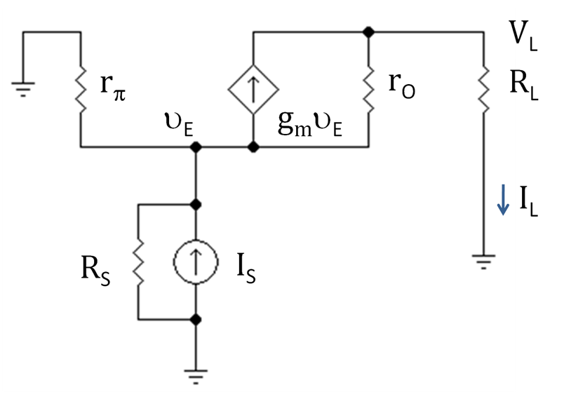
 Figure 3: Common-base circuit with Norton driver; RC is omitted because an active load is assumed with infinite small-signal output resistance
Figure 3 shows the common-base amplifier used as a current follower. The circuit signal is provided by an AC Norton source (current IS, Norton resistance RS) at the input, and the circuit has a resistor load RL at the output.
As mentioned earlier, this amplifier is bilateral as a consequence of the output resistance rO, which connects the output to the input. In this case the output resistance is large even in the worst case (it is at least rO || RC and can become (β + 1) rO || RC for large RS). Large output resistance is a desirable attribute of a current source because favorable current division sends most of the current to the load. The current gain is very nearly unity as long as RS >> rE.
An alternative analysis technique is based upon two-port networks. For example, in an application like this one where current is the output, an h-equivalent two-port is selected because it uses a current amplifier in the output port.
See also
- Two-port networks
- Hybrid-pi model
- Common emitter
- Common collector
- Common source
- Common drain
- Long-tailed pair
References
External links
- Basic BJT Amplifier Configurations
- NPN Common Base Amplifier — HyperPhysics
- ECE 327: Transistor Basics — Gives example common-base circuit (i.e., current source) with explanation.
Transistor amplifiers  Bipolar junction transistor: Common emitter • Common collector • Common base
Field-effect transistor: Common source • Common drain • Common gate
Multiple transistors: Darlington transistor • Sziklai pair • Cascode • Long-tailed pair Categories:
- Single-stage transistor amplifiers

![R_C || \left[ (r_{ \pi}||R_S)(1+g_mr_O) \right]](1/6b1f889a6c96768f9021ebbb66916f9e.png)


Wikimedia Foundation. 2010.