- Diode modelling
-
In electronics, diode modelling refers to the mathematical models used to approximate the actual behavior of real diodes to enable calculations and circuit analysis. A diode's I-V curve is nonlinear (it is well described by the Shockley diode law). This nonlinearity complicates calculations in circuits involving diodes, so simpler models are often required.
This article discusses the modelling of p-n junction diodes, but the techniques may be generalized to other solid state diodes.
Contents
Large-signal modelling
Shockley diode model
The Shockley diode equation relates the diode current I of a p-n junction diode to the diode voltage VD. This relationship is the diode I-V characteristic:
-
 ,
,
where IS is the saturation current or scale current of the diode (the magnitude of the current that flows for negative VD in excess of a few VT, typically 10−12 A). The scale current is proportional to the diode area. Continuing with the symbols: VT is the thermal voltage (kT / q, about 26 mV at normal temperatures), and n is known as the diode ideality factor (for silicon diodes n is approximately 1 to 2).
When
 the formula can be simplified to:
-
 .
.
This expression is, however, only an approximation of a more complex I-V characteristic. Its applicability is particularly limited in case of ultrashallow junctions, for which better analytical models exist.[1]
Diode-resistor circuit example
To illustrate the complications in using this law, consider the problem of finding the voltage across the diode in Figure 1.
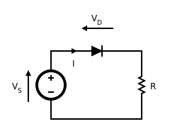 Figure 1: Diode circuit with resistive load.
Because the current flowing through the diode is the same as the current throughout the entire circuit, we can lay down another equation. By Kirchhoff's laws, which boil down to simply Ohm's law in this case, the current flowing in the circuit is
-
 .
.
These two equations determine the diode current and the diode voltage. To solve these two equations, we could substitute the current I from the second equation into the first equation, and then try to rearrange the resulting equation to get VD in terms of VS. A difficulty with this method is that the diode law is nonlinear. Nonetheless, a formula expressing I directly in terms of VS without involving VD can be obtained using the Lambert W-function, which is the inverse function of f(w) = wew, that is, w = W(f). This solution is discussed next.
Explicit solution
An explicit expression for the diode current can be obtained in terms of the Lambert W-function (also called the Omega function). A guide to these manipulations follows. A new variable w is introduced as
-
 .
.
Following the substitutions
 and VD = VS − IR, rearrangement of the diode law in terms of w becomes
-
 ,
,
which using the Lambert W-function becomes
-
 .
.
With the approximations (valid for the most common values of the parameters)
 and
and  , this solution becomes
-
 .
.
Once the current is determined, the diode voltage can be found using either of the other equations.
Iterative solution
The diode voltage VD can be found in terms of VS for any particular set of values by an iterative method using a calculator or computer [2] The diode law is rearranged by dividing by IS, and adding 1. The diode law becomes
-
 .
.
By taking natural logarithms of both sides the exponential is removed, and the equation becomes
-
 .
.
For any I, this equation determines VD. However, I also must satisfy the Kirchhoff's law equation, given above. This expression is substituted for I to obtain
-
 ,
,
or
-
 .
.
The voltage of the source VS is a known given value, but VD is on both sides of the equation, which forces an iterative solution: a starting value for VD is guessed and put into the right side of the equation. Carrying out the various operations on the right side, we come up with a new value for VD. This new value now is substituted on the right side, and so forth. If this iteration converges the values of VD become closer and closer together as the process continues, and we can stop iteration when the accuracy is sufficient. Once VD is found, I can be found from the Kirchhoff's law equation.
Sometimes an iterative procedure depends critically on the first guess. In this example, almost any first guess will do, say
 . Sometimes an iterative procedure does not converge at all: in this problem an iteration based on the exponential function does not converge, and that is why the equations were rearranged to use a logarithm. Finding a convergent iterative formulation is an art, and every problem is different.
Graphical solution
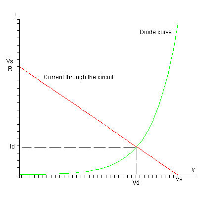
Graphical analysis is a simple way to derive a numerical solution to the transcendental equations describing the diode. As with most graphical methods, it has the advantage of easy visualization. By plotting the I-V curves, it is possible to obtain an approximate solution to any arbitrary degree of accuracy. This process is the graphical equivalent of the two previous approaches, which are more amenable to computer implementation.
This method plots the two current-voltage equations on a graph and the point of intersection of the two curves satisfies both equations, giving the value of the current flowing through the circuit and the voltage across the diode. The following figure illustrates such method.
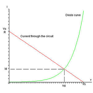 Graphical determination of the operating point through the intersection of the diode characteristic with the resistive load line.
Piecewise linear model
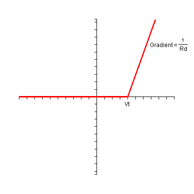
In practice, the graphical method is complicated and impractical for complex circuits. Another method of modelling a diode is called piecewise linear (PWL) modelling. In mathematics, this means taking a function and breaking it down into several linear segments. This method is used to approximate the diode characteristic curve as a series of linear segments. The real diode is modeled as 3 components in series: an ideal diode, a voltage source and a resistor. The figure below shows a real diode I-V curve being approximated by a two-segment piecewise linear model. Typically the sloped line segment would be chosen tangent to the diode curve at the Q-point. Then the slope of this line is given by the reciprocal of the small-signal resistance of the diode at the Q-point.
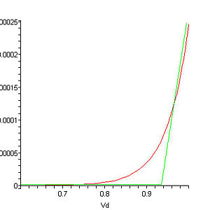 A piecewise linear approximation of the diode characteristic.
Mathematically idealized diode
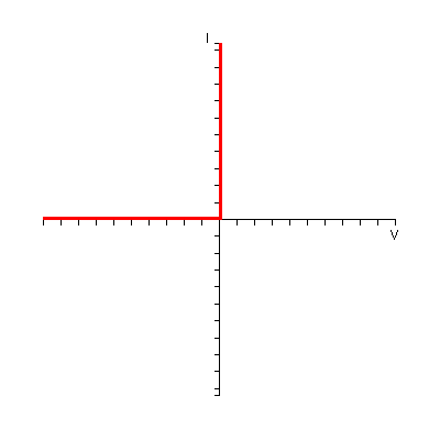
Firstly, let us consider a mathematically idealized diode. In such an ideal diode, if the diode is reverse biased, the current flowing through it is zero. This ideal diode starts conducting at 0 V and for any positive voltage an infinite current flows and the diode acts like a short circuit. The I-V characteristics of an ideal diode are shown below:
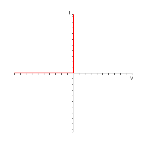 I-V characteristic of an ideal diode.
Ideal diode in series with voltage source
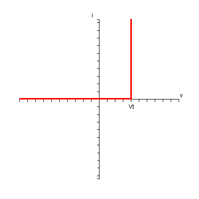
Now let us consider the case when we add a voltage source in series with the diode in the form shown below:
 Ideal diode with a series voltage source.
When forward biased, the ideal diode is simply a short circuit and when reverse biased, an open circuit. If the anode of the diode is connected to 0 V, the voltage at the cathode will be at Vt and so the potential at the cathode will be greater than the potential at the anode and the diode will be reverse biased. In order to get the diode to conduct, the voltage at the anode will need to be taken to Vt. This circuit approximates the cut-in voltage present in real diodes. The combined I-V characteristic of this circuit is shown below:
 I-V characteristic of and ideal diode with a series voltage source.
The Shockley diode model can be used to predict the approximate value of Vt.
Using n = 1 and T = 25C:
Typical values of the saturation current are:
- IS = 10 − 12 for silicon diodes;
- IS = 10 − 6 for germanium diodes.
As the variation of VD goes with the logarithm of the ratio
 , its value varies very little for a big variation of the ratio. The use of base 10 logarithms makes it easier to think in orders of magnitude.
For a current of 1.0 mA:
 for silicon diodes (9 orders of magnitude);
 for germanium diodes (3 orders of magnitude).
For a current of 100 mA:
 for silicon diodes (11 orders of magnitude);
 for germanium diodes (5 orders of magnitude).
Values of 0.6 or 0.7 Volts are commonly used for silicon diodes [3]
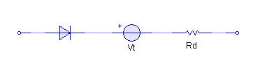
Diode with voltage source and current-limiting resistor
The last thing needed is a resistor to limit the current, as shown below:
 Ideal diode with a series voltage source and resistor.
The I-V characteristic of the final circuit looks like this:
 I-V characteristic of an ideal diode with a series voltage source and resistor.
The real diode now can be replaced with the combined ideal diode, voltage source and resistor and the circuit then is modelled using just linear elements. If the sloped-line segment is tangent to the real diode curve at the Q-point, this approximate circuit has the same small-signal circuit at the Q-point as the real diode.
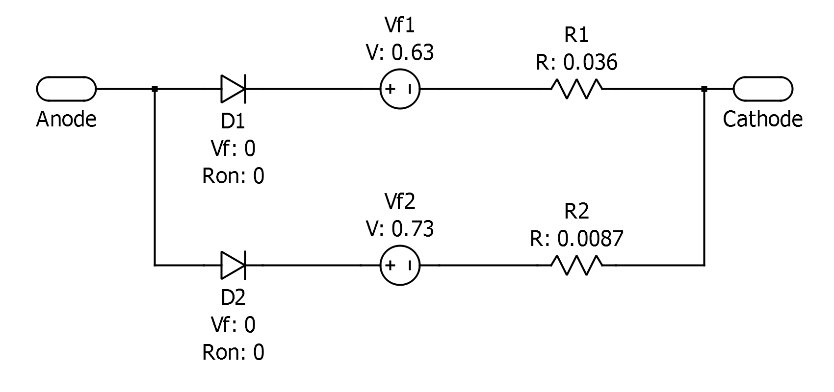
Dual PWL-diodes or 3-Line PWL model
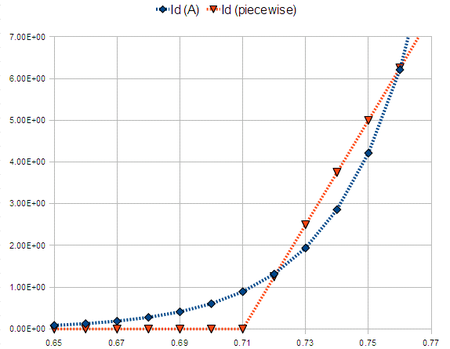 I-V characteristic of the standard PWL model (marked by red-triangles), as described above. Shown for reference is the standard Shockley-diode model (marked by blue-diamonds). The Shockley parameters are Is=1e-12A, Vt=0.0258v
When more accuracy is desired in modeling the diode's turn-on characteristic, the model can be enhanced by doubling-up the standard PWL-model. This model uses two piecewise-linear diodes in parallel, as a way to model a single diode more accurately.
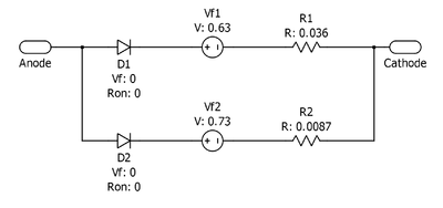 PWL Diode model with 2 branches. The top branch has a lower forward-voltage and a higher resistance. This allows the diode to switch on more gradually, and in this regard more accurately models a real diode. The bottom branch has a higher forward voltage and a lower resistance, thus allowing high current at high voltage
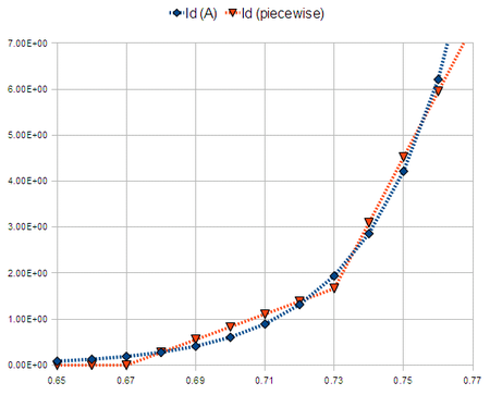 Plot of the I-V Characteristic of this model (marked by red-triangles), as compared to the standard Shockley-diode model (marked by blue-diamonds). The Shockley parameters are Is=1e-12A, Vt=0.0258v
Small-signal modelling
Resistance
Using the Shockley equation, the small-signal diode resistance rD of the diode can be derived about some operating point (Q-point) where the DC bias current is IQ and the Q-point applied voltage is VQ.[4] To begin, the diode small-signal conductance gD is found, that is, the change in current in the diode caused by a small change in voltage across the diode, divided by this voltage change, namely:
-
 .
.
The latter approximation assumes that the bias current IQ is large enough so that the factor of 1 in the parentheses of the Shockley diode equation can be ignored. This approximation is accurate even at rather small voltages, because the thermal voltage
 at 300K, so VQ / VT tends to be large, meaning that the exponential is very large.
Noting that the small-signal resistance rD is the reciprocal of the small-signal conductance just found, the diode resistance is independent of the ac current, but depends on the dc current, and is given as
-
 .
.
Capacitance
The charge in the diode carrying current IQ is known to be
- Q = IQτF + QJ,
where τF is the forward transit time of charge carriers:[4] The first term in the charge is the charge in transit across the diode when the current IQ flows. The second term is the charge stored in the junction itself when it is viewed as a simple capacitor; that is, as a pair of electrodes with opposite charges on them. It is the charge stored on the diode by virtue of simply having a voltage across it, regardless of any current it conducts.
In a similar fashion as before, the diode capacitance is the change in diode charge with diode voltage:
-
 ,
,
where
 is the junction capacitance and the first term is called the diffusion capacitance, because it is related to the current diffusing through the junction.
References
- ^ . Popadic, Milo¿; Lorito, Gianpaolo; Nanver, Lis K. (2009). "Analytical Model of I – V Characteristics of Arbitrarily Shallow p-n Junctions". IEEE Transactions on Electron Devices 56: 116–125. doi:10.1109/TED.2008.2009028. http://ieeexplore.ieee.org/search/srchabstract.jsp?arnumber=4717238&isnumber=4723893&punumber=16&k2dockey=4717238@ieeejrns&query=%28+%28%28electron+devices%29%3Cin%3Emetadata+%29+%3Cand%3E+%28%28popadic%29%3Cin%3Emetadata+%29+%29&pos=0&access=no.
- ^ . A.S. Sedra and K.C. Smith (2004). Microelectronic Circuits (Fifth ed.). New York: Oxford. Example 3.4 p. 154. ISBN 0-19-514251-9. http://worldcat.org/isbn/0195142519.
- ^ . Kal, Santiram (2004). "Chapter 2". Basic Electronics: Devices, Circuits and IT Fundamentals (Section 2.5: Circuit Model of a P-N Junction Diode ed.). Prentice-Hall of India Pvt.Ltd. ISBN 8120319524.
- ^ a b R.C. Jaeger and T.N. Blalock (2004). Microelectronic Circuit Design (second ed.). McGraw-Hill. ISBN 0-07-232099-0. http://books.google.com/?id=u6vH4Gsrlf0C&pg=PA883&dq=%22Microelectronic+Circuit+Design%22+inauthor:Jaeger+small-signal+diode.
See also
Categories:- Electronic device modeling
-


Wikimedia Foundation. 2010.