- Nanowire
-
Part of a series of articles on
Single-molecule electronics Molecular scale electronics
Molecular logic gate
Molecular wiresSolid state nanoelectronics Nanocircuitry
Nanowires
Nanolithography
NEMS
NanosensorRelated approaches See also
Nanotechnology
A nanowire is a nanostructure, with the diameter of the order of a nanometer (10−9 meters). Alternatively, nanowires can be defined as structures that have a thickness or diameter constrained to tens of nanometers or less and an unconstrained length. At these scales, quantum mechanical effects are important — which coined the term "quantum wires". Many different types of nanowires exist, including metallic (e.g., Ni, Pt, Au), semiconducting (e.g., Si, InP, GaN, etc.), and insulating (e.g., SiO2, TiO2). Molecular nanowires are composed of repeating molecular units either organic (e.g. DNA) or inorganic (e.g. Mo6S9-xIx).
The nanowires could be used, in the near future, to link tiny components into extremely small circuits. Using nanotechnology, such components could be created out of chemical compounds.
Contents
Overview
Typical nanowires exhibit aspect ratios (length-to-width ratio) of 1000 or more. As such they are often referred to as one-dimensional (1-D) materials. Nanowires have many interesting properties that are not seen in bulk or 3-D materials. This is because electrons in nanowires are quantum confined laterally and thus occupy energy levels that are different from the traditional continuum of energy levels or bands found in bulk materials.
Peculiar features of this quantum confinement exhibited by certain nanowires manifest themselves in discrete values of the electrical conductance. Such discrete values arise from a quantum mechanical restraint on the number of electrons that can travel through the wire at the nanometer scale. These discrete values are often referred to as the quantum of conductance and are integer values of
They are inverse of the well-known resistance unit h/e2, which is roughly equal to 25812.8 ohms, and referred to as the von Klitzing constant RK (after Klaus von Klitzing, the discoverer of exact quantization). Since 1990, a fixed conventional value RK-90 is accepted.[1]
Examples of nanowires include inorganic molecular nanowires (Mo6S9-xIx, Li2Mo6Se6), which can have a diameter of 0.9 nm and be hundreds of micrometers long. Other important examples are based on semiconductors such as InP, Si, GaN, etc., dielectrics (e.g. SiO2,TiO2), or metals (e.g. Ni, Pt).
There are many applications where nanowires may become important in electronic, opto-electronic and nanoelectromechanical devices, as additives in advanced composites, for metallic interconnects in nanoscale quantum devices, as field-emitters and as leads for biomolecular nanosensors.
Synthesis of nanowires
 An SEM image of epitaxial nanowire heterostructures grown from catalytic gold nanoparticles.
There are two basic approaches of synthesizing nanowires: top-down and bottom-up approach. In a top-down approach a large piece of material is cut down to small pieces through different means such as lithography and electrophoresis. Whereas in a bottom-up approach the nanowire is synthesized by the combination of constituent ad-atoms. Most of the synthesis techniques are based on bottom-up approach.
Nanowire structures are grown through several common laboratory techniques including suspension, deposition (electrochemical or otherwise), and VLS growth. Ion track technology enables growing homogeneous and segmented nanowires down to 8 nm diameter.
Suspension
A suspended nanowire is a wire produced in a high-vacuum chamber held at the longitudinal extremities. Suspended nanowires can be produced by:
- The chemical etching, or bombardment (typically with highly energetic ions) of a larger wire
- Indenting the tip of a STM in the surface of a metal near its melting point, and then retracting it
VLS Growth
A common technique for creating a nanowire is the Vapor-Liquid-Solid (VLS) synthesis method. This technique uses as source material either laser ablated particles or a feed gas (such as silane). The source is then exposed to a catalyst. For nanowires, the best catalysts are liquid metal (such as gold) nanoclusters, which can either be purchased in colloidal form and deposited on a substrate or self-assembled from a thin film by dewetting. This process can often produce crystalline nanowires in the case of semiconductor materials.
The source enters these nanoclusters and begins to saturate it. Once supersaturation is reached, the source solidifies and grows outward from the nanocluster. The final product's length can be adjusted by simply turning off the source. Compound nanowires with super-lattices of alternating materials can be created by switching sources while still in the growth phase.
Inorganic nanowires such as Mo6S9-xIx(which are alternatively viewed as cluster polymers) are synthesised in a single-step vapour phase reaction at elevated temperature.
Solution-phase synthesis
Nanowires of many types of materials can be grown in solution. Solution-phase synthesis has the advantage that it can be scaled-up to produce very large quantities of nanowires as compared to methods that produce nanowires on a surface. The polyol synthesis, in which ethylene glycol is both solvent and reducing agent, has proven particularly versatile at producing nanowires of Pb, Pt, and silver.
Physics of nanowires
Conductivity of nanowires
 An SEM image of a 15 micrometre nickel wire.
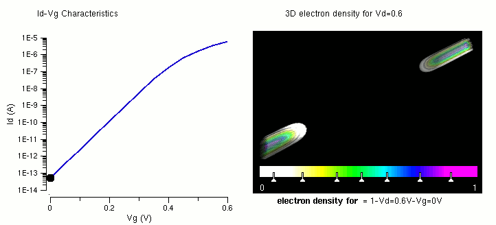
 Atomistic simulation result for formation of inversion channel (electron density) and attainment of threshold voltage (IV) in a nanowire MOSFET. Note that the threshold voltage for this device lies around 0.45V.
The conductivity of a nanowire is expected to be much less than that of the corresponding bulk material. This is due to a variety of reasons. First, there is scattering from the wire boundaries, when the wire width is below the free electron mean free path of the bulk material. In copper, for example, the mean free path is 40 nm. Nanowires less than 40 nm wide will shorten the mean free path to the wire width.
Nanowires also show other peculiar electrical properties due to their size. Unlike carbon nanotubes, whose motion of electrons can fall under the regime of ballistic transport (meaning the electrons can travel freely from one electrode to the other), nanowire conductivity is strongly influenced by edge effects. The edge effects come from atoms that lay at the nanowire surface and are not fully bonded to neighboring atoms like the atoms within the bulk of the nanowire. The unbonded atoms are often a source of defects within the nanowire, and may cause the nanowire to conduct electricity more poorly than the bulk material. As a nanowire shrinks in size, the surface atoms become more numerous compared to the atoms within the nanowire, and edge effects become more important.
Furthermore the conductivity can undergo a quantization in energy: i.e. the energy of the electrons going through a nanowire can assume only discrete values, multiple of the Von Klitzing constant G = 2e2/h (where e is the charge of the electron and h is the Planck constant).
The conductivity is hence described as the sum of the transport by separate channels of different quantized energy levels. The thinner the wire is, the smaller the number of channels available to the transport of electrons.
The conductivity of a nanowire can be studied suspending it between two electrodes. This has been proven by measuring the conductivity of a nanowire while pulling it: as its diameter is reduced, its conductivity decreases in a stepwise fashion and the plateaus correspond to multiples of G.
The quantized conductivity is more pronounced in semiconductors like Si or GaAs than in metals, due to lower electron density and lower effective mass. Quantized conductance can be observed in 25 nm wide silicon fins, resulting in increased threshold voltage.[2]
Welding nanowires
To incorporate nanowire technology into industrial applications, researchers in 2008 developed a method of welding nanowires together: a sacrificial metal nanowire is placed adjacent to the ends of the pieces to be joined (using the manipulators of a scanning electron microscope); then an electric current is applied, which fuses the wire ends. The technique fuses wires as small as 10 nm.[3]
For nanowires with diameters less than 10 nm, existing welding techniques, which requiring precise control of the heating mechanism and may introducing the possibility of damage, will be not practical. Recently scientists discovered that single-crystalline ultrathin gold nanowires with diameters ~3-10 nm can be "cold-welded" together within seconds by mechanical contact alone, and under remarkably low applied pressures (unlike macro- and micro-scale cold welding process).[4] High-resolution transmission electron microscopy and in situ measurements reveal that the welds are nearly perfect, with the same crystal orientation, strength and electrical conductivity as the rest of the nanowire. The high quality of the welds is attributed to the nanoscale sample dimensions, oriented-attachment mechanisms and mechanically assisted fast surface diffusion. Nanowire welds were also demonstrated between gold and silver, and silver and silver nanowires (with diameters ~5-15 nm) at near room temperature, indicating that this technique may be generally applicable for ultrathin metallic nanowires. Combined with other nano- and microfabrication technologies,[5][6] cold welding is anticipated to have potential applications in the future bottom-up assembly of metallic one-dimensional nanostructures.
Uses of nanowires
Nanowires still belong to the experimental world of laboratories. However, they may complement or replace carbon nanotubes in some applications. Some early experiments have shown how they can be used to build the next generation of computing devices.
To create active electronic elements, the first key step was to chemically dope a semiconductor nanowire. This has already been done to individual nanowires to create p-type and n-type semiconductors.
The next step was to find a way to create a p-n junction, one of the simplest electronic devices. This was achieved in two ways. The first way was to physically cross a p-type wire over an n-type wire. The second method involved chemically doping a single wire with different dopants along the length. This method created a p-n junction with only one wire.
After p-n junctions were built with nanowires, the next logical step was to build logic gates. By connecting several p-n junctions together, researchers have been able to create the basis of all logic circuits: the AND, OR, and NOT gates have all been built from semiconductor nanowire crossings.
It is possible that semiconductor nanowire crossings will be important to the future of digital computing. Though there are other uses for nanowires beyond these, the only ones that actually take advantage of physics in the nanometer regime are electronic.
Nanowires are being studied for use as photon ballistic waveguides as interconnects in quantum dot/quantum effect well photon logic arrays. Photons travel inside the tube, electrons travel on the outside shell.
When two nanowires acting as photon waveguides cross each other the juncture acts as a quantum dot.
Conducting nanowires offer the possibility of connecting molecular-scale entities in a molecular computer. Dispersions of conducting nanowires in different polymers are being investigated for use as transparent electrodes for flexible flat-screen displays.
Because of their high Young's moduli, their use in mechanically enhancing composites is being investigated. Because nanowires appear in bundles, they may be used as tribological additives to improve friction characteristics and reliability of electronic transducers and actuators.
Because of their high aspect ratio, nanowires are also uniquely suited to dielectrophoretic manipulation.[7][8]
See also
- Carbon nanotubes
- Inorganic nanotubes
- Molecular nanowires
- Nanoantenna
- Nanorods
- Nanowire battery
- Solar cell
- Quantum Hall effect
References
- ^ von Klitzing constant
- ^ A. T. Tilke et al. (2003). Physical Rev. B 68: 075311.
- ^ Wee Welding with Nanosolder, Chemical & Engineering News, 86, 51 (22 Dec. 2008), p. 35
- ^ Cold welding of ultrathin gold nanowires, Nature Nanotechnology, Y. Lu et al. 5, (14 Feb. 2010, doi:10.1038/nnano.2010.4), p. 213-224
- ^ Nanowire crossbar arrays as address decoders for integrated nanosystems, Science, Zhong, Z., Wang, D., Cui, Y., Bockrath, M. W. & Lieber, C. M. 302, (2003), p. 1377
- ^ Polymer pen lithography, Science, F. Huo et al. 321, (2008), p. 1658-1660
- ^ "Nanowires get reconfigured". October 19, 2006. http://nanotechweb.org/articles/journal/5/10/2/1.
- ^ Grange, R.; Choi, J.W.; Hsieh, C.L.; Pu, Y.; Magrez, A.; Smajda, R.; Forro, L.; Psaltis, D. (2009). "Lithium niobate nanowires: synthesis, optical properties and manipulation". Applied Physics Letters 95: 143105. http://link.aip.org/link/?APPLAB/95/143105/1.
Further reading
- K. v. Klitzing, G. Dorda, and M. Pepper; Phys. Rev. Lett. 45, 494-497 (1980)[1]
- R. Landauer, J. Phys.: Cond. Matter 1, 8099 (1989) [2]
- N. Oncel et al., Phys. Rev. Lett. 95, 116801, (2005)
- J. Chen, B. Wiley, Y. Xia. One-Dimensional Nanostructures of Metals: Large-Scale Synthesis and Some Potential Applications. Langmuir 2007, 23, 4120.
- Ross, Frances M., "Controlling nanowire structures through real time growth studies", Reports on Progress in Physics, Volume 73, Number 11, 2010
- Bullis, Kevin, "Nanowire Transistors Faster than Silicon", MIT Technology Review, June 20, 2006
External links
- Nanohedron.com | Nano Image Gallery several images of nanowires are included in the galleries.
- Stanford's nanowire battery holds 10 times the charge of existing ones
- Original article on the Quantum Hall Effect: K. v. Klitzing, G. Dorda, and M. Pepper; Phys. Rev. Lett. 45, 494-497 (1980).
- Strongest theoretical nanowire produced at Australia's University of Melbourne.
- Penn Engineers Design Electronic Computer Memory in Nanoscale Form That Retrieves Data 1,000 Times Faster.
- One atom thick, hundreds of nanometers long Pt-nanowires are one of the best examples of self-assembly. (University of Twente)
Categories:- Nanoelectronics
- Electrical connectors


Wikimedia Foundation. 2010.