- Deep-level transient spectroscopy
-
Deep Level Transient Spectroscopy (DLTS) is an experimental tool for studying electrically active defects (known as charge carrier traps) in semiconductors. DLTS establishes fundamental defect parameters and measures their concentration in the material. Some of the parameters are considered as defect “finger prints” used for their identifications and analysis.
DLTS investigates defects present in a space charge (depletion) region of a simple electronic device. The most commonly used are Schottky diodes or p-n junctions. In the measurement process the steady-state diode reverse polarization voltage is disturbed by a voltage pulse. This voltage pulse reduces the electric field in the space charge region and allows free carriers from the semiconductor bulk to penetrate this region and recharge the defects causing their non-equilibrium charge state. After the pulse, when the voltage returns to its steady-state value, the defects start to emit trapped carriers due to the thermal emission process. The technique observes the device space charge region capacitance where the defect charge state recovery causes the capacitance transient. The voltage pulse followed by the defect charge state recovery are cycled allowing an application of different signal processing methods for defect recharging process analysis.
The DLTS technique has a higher sensitivity than almost any other semiconductor diagnostic technique. For example, in silicon it can detect impurities and defects at a concentration of one part in 1012 of the material host atoms. This feature together with a technical simplicity of its design made it very popular in research labs and semiconductor material production factories.
The DLTS technique was pioneered by D. V. Lang (David Vern Lang of Bell Laboratories) in 1974.[1] US Patent[2] was awarded to Lang in 1975.
Contents
DLTS methods
Conventional DLTS
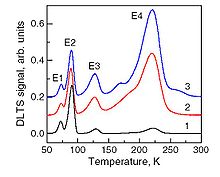 Typical conventional DLTS spectra
In conventional DLTS the capacitance transients are investigated by using a lock-in amplifier or double box-car averaging technique when the sample temperature is slowly varied (usually in a range from liquid nitrogen temperature to room temperature 300K or above). The equipment reference frequency is the voltage pulse repetition rate. In the conventional DLTS method this frequency multiplied by some constant (depending on the hardware used) is called the “rate window”. When during the sample temperature variation the emission rate of carriers from some defect equals to the rate window one obtains in the spectrum a peak. By setting up different rate windows in subsequent DLTS spectra measurements one obtains different temperatures at which some particular peak appears. Having a set of the emission rate and corresponding temperature pairs one can make an Arrhenius plot which allows for the deduction of defect activation energy for the thermal emission process. Usually this energy (sometimes called the defect energy level) together with the plot intersect value are defect parameters used for its identification or analysis.
Recently, DLTS has been used to study quantum dots.[3][4][5]
MCTS and minority-carrier DLTS
For the Schottky diodes, majority carrier traps are observed by the application of a reverse bias pulse, while minority carrier traps can be observed when the reverse bias voltage pulses are replaced with light pulses with the photon energy from the above semiconductor bandgap spectral range.[6][7] This method is called Minority Carrier Transient Spectroscopy (MCTS). The minority carrier traps can be also observed for the p-n junctions by application of forward bias pulses which inject minority carriers into the space charge region.[8] In DLTS plots the minority carrier spectra usually are depicted with an opposite sign of amplitude in respect to the majority carrier trap spectra.
Laplace DLTS
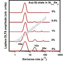 Typical Laplace DLTS spectra: atom of gold in SiGe crystals
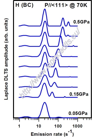
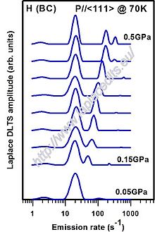 The uniaxial-stress Laplace DLTS measurements: interstitial atom of hydrogen in silicon
There is an extension to DLTS known as a high resolution Laplace transform DLTS (LDLTS). Laplace DLTS is an isothermal technique in which the capacitance transients are digitized and averaged at a fixed temperature. Then the defect emission rates are obtained with a use of numerical methods being equivalent to the inverse Laplace transformation. The obtained emission rates are presented as a spectral plot.[9][10] The main advantage of Laplace DLTS in comparison to conventional DLTS is the substantial increase in energy resolution understood here as an ability to distinguish very similar signals.
Laplace DLTS in combination with uniaxial stress results in a splitting of the defect energy level. Assuming a random distribution of defects in non-equivalent orientations, the number of split lines and their intensity ratios reflect the symmetry class[11] of the given defect.[9]
Application of LDLTS to MOS capacitors needs device polarization voltages in a range where the Fermi level extrapolated from semiconductor to the semiconductor-oxide interface intersects this interface within the semiconductor bandgap range. The electronic interface states present at this interface can trap carriers similarly to defects described above. If their occupancy with electrons or holes is disturbed by a small voltage pulse then the device capacitance recovers after the pulse to its initial value as the interface states start to emit carriers. This recovery process can be analyzed with the LDLTS method for different device polarization voltages. Such a procedure allows to obtain the energy state distribution of the interface electronic states at the semiconductor-oxide (or dielectric) interfaces.[12]
Constant-Capacitance DLTS
In general, the analysis of the capacitance transients in the DLTS measurements assumes that the concentration of investigated traps is much smaller than the material doping concentration. In cases when this assumption is not fulfilled then the constant capacitance DLTS (CCDLTS) method is used for more accurate determination of the trap concentration.[13] When the defects recharge and their concentration is high then the width of the device space region varies making the analysis of the capacitance transient inaccurate. The additional electronic circuitry maintaining the total device capacitance constant by varying the device bias voltage helps to keep the depletion region width constant. As a result, the varying device voltage reflects the defect recharge process. An analysis of the CCDLTS system using feedback theory was provided by Lau and Lam in 1982.[14]
I-DLTS and PITS
There is an important shortcoming for DLTS: it cannot be used for insulating materials. (Note: an insulator can be considered as a very large bandgap semiconductor.) For insulating materials it is difficult or impossible to produce a device having a space region which width could be changed by the external voltage bias and thus the capacitance measurement-based DLTS methods cannot be applied for the defect analysis. Basing on experiences of the thermally stimulated current (TSC) spectroscopy, the current transients are analyzed with the DLTS methods (I-DLTS), where the light pulses are used for the defect occupancy disturbance. This method in the literature is sometimes called the Photoinduced Transient Spectroscopy (PITS).[15] I-DLTS or PITS are also used for studying defects in the i-region of a p-i-n diode.
See also
- Carrier generation and recombination
- Bandgap
- Effective mass
- Schottky diode
- Frenkel defect
- Schottky defect
- Semiconductor device
- Vacancy (chemistry)
- Capacitance voltage profiling
- High-k dielectric
References
- ^ D.V. Lang, "Deep-level transient spectroscopy: A new method to characterize traps in semiconductors", J. Appl. Phys., vol. 45 (1974) 3023.
- ^ US Patent 3,859,595
- ^ S. W. Lin, C. Balocco, M. Missous, A. R. Peaker, and A. M. Song, Phys. Rev. B 72, 165302 (2005).
- ^ I.V. Antonova, V.A. Volodin, E.P. Neustroev, S. A. Smagulova, J. Jedrzejewsi, and I. Balberg, J. Appl. Phys. 106, 064306 (2009).
- ^ M. Buljan, J. Grenzer, V. Holý, N. Radić, T. Mišić-Radić, S. Levichev, S. Bernstorff, B. Pivac, and I. Capan, Appl. Phys. Lett. 97, 163117 (2010)
- ^ R. Brunwin et al. “Detection of minority-carrier traps using transient spectroscopy” Electronics Letters, vol. 15 (1979) 349
- ^ B. Hamilton et al. “Deep-state-controlled minority-carrier lifetime in n-type gallium phosphide” J. Appl. Phys. vol. 50, (1979) 6373
- ^ V.P. Markevich et al., "Vacancy–group-V-impurity atom pairs in Ge crystals doped with P, As, Sb, and Bi ", Phys. Rev. B, vol. 70 (2004) 235213.
- ^ a b L. Dobaczewski, A. R. Peaker, and K. Bonde Nielsen, “Laplace-transform deep-level spectroscopy: the technique and its applications to the study of point defects in semiconductors”, J. Appl. Phys. (Applied Physics Reviews), vol. 96 (2004) 4689
- ^ Laplace transform Deep Level Transient Spectroscopy
- ^ Point Group Symmetry
- ^ L. Dobaczewski et al., “Energy-state distributions of the Pb centers at the (100), (110), and (111) Si/SiO2 interfaces investigated by Laplace Deep Level Transient Spectroscopy”, Appl. Phys. Lett, vol. 92 (2008) 242104
- ^ N.M. Johnson, D.J. Bartelink, R.B. Gold and J.F. Gibbons, "Constant-capacitance DLTS measurement of defect-density profiles in semiconductos", J. Appl. Phys., vol. 50, (1079) 4828.
- ^ W.S. Lau and Y.W. Lam, "Analysis of and some design considerations for the constant capacitance DLTS system", International Journal of Electronics, vol. 52(1982) 369
- ^ C. Hurtes, M. Boulou, A. Mitonneau, and D. Bois, "Deep-level spectroscopy in high-resistivity materials", Appl. Phys. Lett. vol. 32 (1978) 821
External links
Categories:- Semiconductor analysis
- Spectroscopy


Wikimedia Foundation. 2010.