- Electron backscatter diffraction
-
 An electron backscatter diffraction pattern
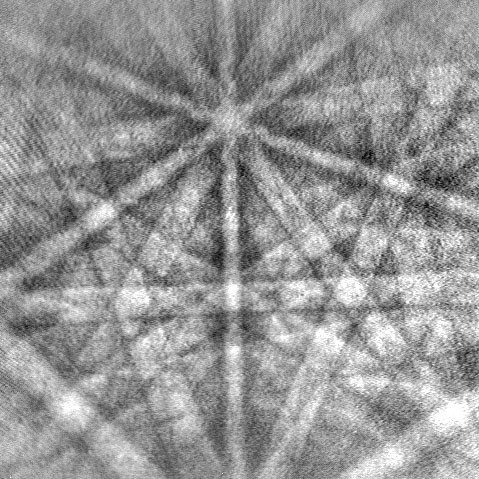
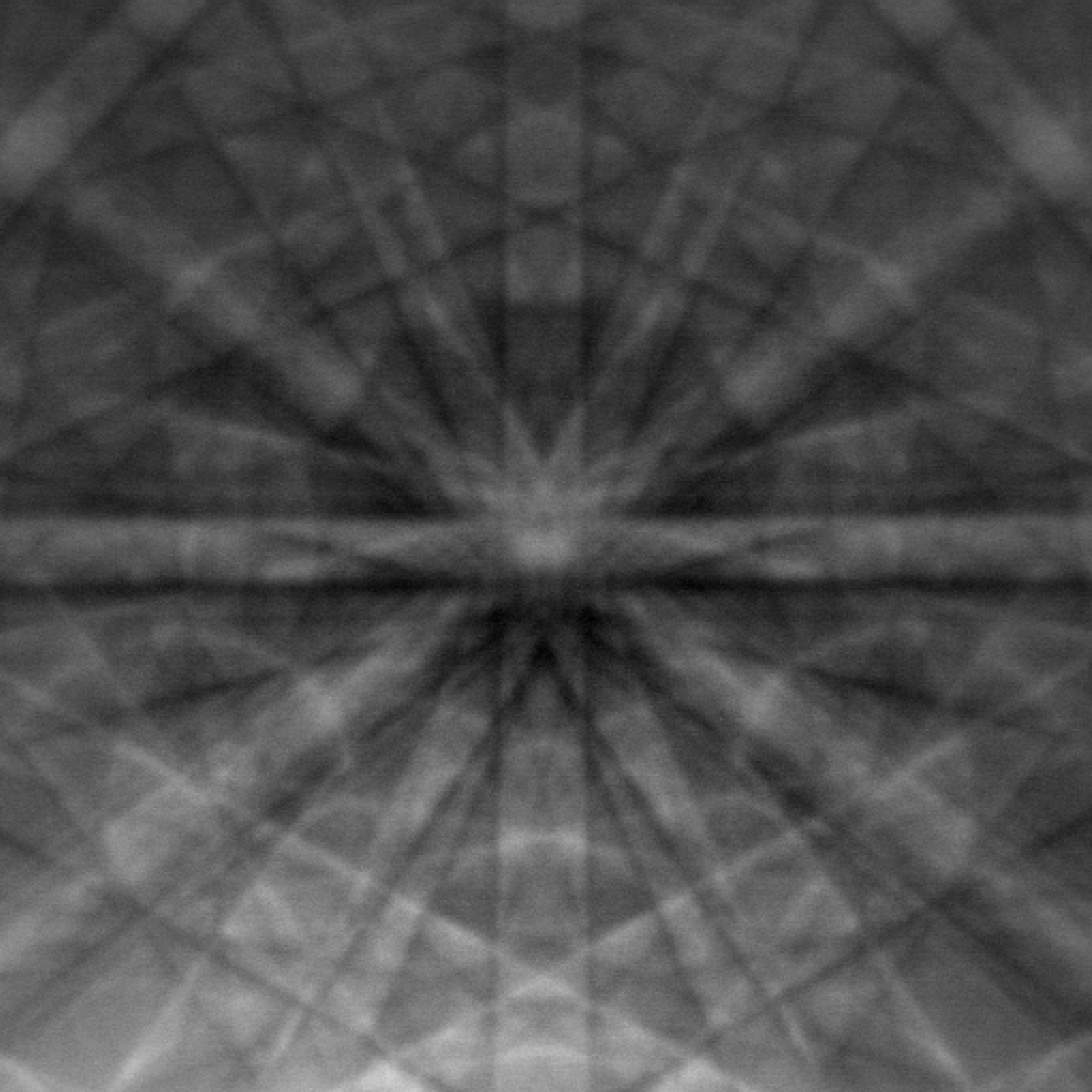
 An electron backscatter diffraction pattern of monocrystalline silicon, taken at 20 kV with a field-emission electron source
Electron backscatter diffraction (EBSD), also known as backscatter Kikuchi diffraction (BKD) is a microstructural-crystallographic technique used to examine the crystallographic orientation of many materials, which can be used to elucidate texture or preferred orientation of any crystalline or polycrystalline material. EBSD can be used to index and identify the seven crystal systems, and as such it is applied to crystal orientation mapping, defect studies, phase identification, grain boundary and morphology studies, regional heterogeneity investigations, material discrimination, microstrain mapping, and using complementary techniques, physico-chemical identification. Traditionally these types of studies have been carried out using X-ray diffraction (XRD), neutron diffraction and/or electron diffraction in a TEM.
Experimentally EBSD is conducted using a Scanning Electron Microscope (SEM) equipped with an EBSD detector containing at least a phosphor screen, compact lens and low light CCD camera chip. Commercially available EBSD systems typically come with one of two different CCD cameras: for fast measurements the CCD chip has a native resolution of 640x480 pixels; for slower, and more sensitive measurements, the CCD chip resolution can go up to 1600x1200 pixels. However, with higher resolutions the readouts are more time-consuming. The biggest advantage of the high-resolution detectors is their higher sensitivity. For texture and orientation measurements, the images are binned in order to reduce their size and reduce computational times. Thus, the transfer and interpretation of up to 880 images/s is possible if the diffraction signal is sufficient [1] .
For an EBSD measurement a flat/polished crystalline specimen is placed in the SEM chamber at a highly tilted angle (~70° from horizontal) towards the diffraction camera (to increase the contrast in the resultant electron backscatter diffraction pattern). The phosphor screen is located within the specimen chamber of the SEM at an angle off approximately 90° to the pole piece and is coupled to a compact lens which focusses the image from the phosphor screen onto the CCD camera. Electrons can backscatter within the material as these backscattering electrons exit the crystal they may exit at the Bragg condition related to the spacing of the periodic atomic lattice planes of the crystalline structure. These diffracted electrons can escape the material and some will collide and excite the phosphor causing it to fluoresce.
An electron backscatter diffraction pattern (EBSP) is formed when many different planes diffract different electrons to form kikuchi bands which correspond to each of the lattice diffracting planes. If the system geometry is well described, it is possible to relate the bands present in the EBSP to the underlying crystal phase and orientation of the material within the electron interaction volume. Each band can be indexed individually by the Miller indices of the diffracting plane which formed it. In most materials, only three bands/planes which intercept are required to describe a unique solution to the crystal orientation (based upon their interplanar angles) and most commercial systems use look up tables with international crystal data bases to perform indexing.
While this 'geometric' description related to the kinematic solution (using the Bragg condition) is very powerful and useful for orientation and texture analysis, it only describes the geometry of the crystalline lattice and ignores many physical processes involved within the diffracting material. To adequately describe finer features within the EBSP, one must use a many beam dynamical model (e.g. the variation in band intensities in an experimental pattern does not fit the kinematic solution related to the structure factor).
Contents
Indexing
Often, the first step in the EBSD process after pattern collection is indexing. This allows for identification of the crystal orientation at the single volume of the sample from where the pattern was collected. With EBSD software, pattern bands are typically detected via a mathematical routine called the Hough transform, in which every pixel in Hough space denotes a unique line/band in the EBSP. The Hough transform is used to enable band detection, which are difficult to locate by computer in the original EBSP. Once the band locations have been detected it is possible to relate these locations to the underlying crystal orientation, as angles between bands represent angles between lattice planes. Thus when the position / angles between three bands are known an orientation solution can be determined. In highly symmetric materials typically more than three bands are utilised to obtain and verify the orientation measurement.
There are two leading methods of indexing performed by most commercial EBSD software: triplet voting; and minimising the 'fit' between the experimental pattern and a computationally determined orientation.
Triplet voting involves identify multiple 'triplets' associated with different solutions to the crystal orientation; each crystal orientation determined from each triplet receives one vote. Should four bands identify the same crystal orientation then four (four choose three) votes will be cast for that particular solution. Thus the candidate orientation with the highest number of votes will be the most likely solution to the underlying crystal orientation present. The ratio of votes for the solution chosen as compared to the total number of votes describes the confidence in the underlying solution. Care must be taken in interpreting this 'confidence index' as some pseudo-symmetric orientations may result in low confidence for one candidate solution vs. another.
Minimising the fit involves starting with all possible orientations for a triplet. More bands are included that reduces the number of candidate orientations. As the number of bands increases, the number of possible orientations converge ultimately to one solution. The 'fit' between the measured orientation and the captured pattern can be determined.
Pattern Centre
In order to relate the orientation of a crystal, much like in X-ray diffraction, the geometry of the system must be known. In particular the pattern centre, which describes both the distance of the interaction volume to the detector and the location of the nearest point between the phosphor and the sample on the phosphor screen. Early work utilised a single crystal of known orientation being inserted into the SEM chamber and a particular feature of the EBSP was known to correspond to the pattern centre. Later developments involved exploiting various geometric relationships between the generation of an EBSP and the chamber geometry (shadow casting and phosphor movement).
Unfortunately each of these methods are cumbersome, prone to some systematic errors for a general operator and can not be easily utilised in modern SEMs with multiple designated uses. Thus most commercial EBSD systems utilise the indexing algorithm combined with an iterative movement of both crystal orientation and suggested pattern centre location. Minimising the fit between bands located within experimental patterns and those in look up tables tends to converge on the pattern centre location to an accuracy of ~0.5–1% of the pattern width.
Orientation mapping
EBSD can be used to find the crystal orientation of the material located within the incident electron beam's interaction volume. Thus by scanning the electron beam in a prescribed fashion (typically in a square or hexagonal grid, correcting for the image foreshortening due to the sample tilt) results in many maps.
These maps can spatially describe the crystal orientation of the material being interrogated and can be used to examine microtexture and sample morphology. Some of these maps describe grain orientation, grain boundary, image quality. Various statistical tools can be used to measure the average misorientation, grain size, and crystallographic texture. From this dataset numerous maps, charts and plots can be generated.
From orientation data, a wealth of information can be devised that aids in the understanding of the samples microstructure and processing history. Recent developments include understanding: the prior texture of parent phases at elevated temperature; the storage and residual deformation after mechanical testing; the population of various microstructural features, including precipitates and grain boundary character.
Integrated EBSD/EDS mapping
When simultaneous EDS/EBSD collection can be achieved, the capabilities of both techniques can be enhanced. There are applications where sample chemistry or phase cannot be differentiated via EDS alone because of similar composition; and structure cannot be solved with EBSD alone because of ambiguous structure solutions. To accomplish integrated mapping, analysis area is scanned and at each point Hough peaks and EDS region-of-interest counts are stored. Positions of phases are determined in X-ray maps and measured EDS intensities are given in charts for each element. For each phase the chemical intensity ranges are set to select the grains. All patterns are then re-indexed off-line. The recorded chemistry determines which phase / crystal structure file is used for indexing of each point. Each pattern is indexed by only one phase and maps displaying clearly distinguished phases are generated.
EBSD when used together with other in-SEM techniques such as cathodoluminescence (CL), wavelength dispersive X-ray spectroscopy (WDS) and/or energy dispersive X-ray spectroscopy (EDS) can provide a deeper insight into the specimen's properties. For example, the minerals calcite (limestone) and aragonite (shell) have the same chemical composition – calcium carbonate (CaCO3) therefore EDS/WDS cannot tell them apart, but they have different microcrystalline structures so EBSD can differentiate between them.
See also
References
- ^ "e–Flash 1000 EBSD Detector". http://www.bruker-axs.com/e-flash-ebsd0.html. Retrieved 13 September 2011.
Categories:- Scientific techniques
- Diffraction
- Spectroscopy
Wikimedia Foundation. 2010.